Popular in 1979-1980, the Ohio Scientific Superboard II was a single-board computer complete with keyboard, video output, and running the BASIC computer language. Its low price attracted a lot of experimenters and hobbyists interested in getting into computers, including myself since this was (in 1979) my first real computer.
Ohio Scientific
Ohio Scientific, Inc (OSI) started business in 1975 and through the late 1970’s and early 1980’s produced a series of 6502-based machines called the “Challenger” series.
Like many contemporaries (including the Apple and the Commodore machines), OSI systems used the low-cost 6502 processor. Created as a low-cost response to Motorola’s 6800 processor, and commercially available (in production quantities) in 1976, the 6502 could use all readily-available and inexpensive 6800 peripheral chips (as OSI did to save cost – 65xx peripheral chips were considerably more expensive). The 6502 achieved low costs through a number of design features including the fabrication in NMOS technology and use of “zero-page” memory which allowed reduction of the number of on-chip registers to six. The 6502, in a design reminiscent of the PDP-8 processor from two decades earlier, allows fast access to the first 256 bytes of RAM from most instructions (making the 6502 almost RISC-like). The next 256 bytes (0x100 through 0x1FF) are prewired as the stack. All 6502 systems, therefore, require at least 512 bytes of RAM located in the lowest memory page and unlike the contemporary Z-80 processor, programs cannot simply be located at address zero (the 6502 actually fetches a vector for the start program from the highest two bytes – a ROM must be located there).
By 1977, OSI offered several models of computers all based on a single-board CPU, the model 500 card. This card featured 8K BASIC-in-ROM (2Kx8 chips), 4K of RAM on board (thirty-two 2102 1Kx1 chips), and a serial port interface. One side of the card featured connectors allowing it to plug into a backplane for expansion by adding other cards such as video, memory, and floppy however it could be used as a standalone system, the C2-0 Model 500 Board ($298), with the user required to add a power supply and a serial terminal for a basic system. The C-28K 500 Superkit ($398) consisted of the basic model 500 CPU board, again with 4K RAM and 8K BASIC-in-ROM, along with a 480 8-slot backplane and 440 video board (with 32 by 32 character display) allowing use with a video monitor instead of a terminal. It was an unpackaged, “open” system in which the user added a power supply and an external ASCII parallel keyboard for a complete system.
Challenger-II systems using the 500 CPU was also available as ‘packaged’ versions in a box with a power supply. The smallest system (the C2-4P outlined on another page on this site) had 4 slots and used cassette storage while the largest systems featured dual eight-inch floppy drives in a separate box and were priced at $2000 to $3000.
In 1979 OSI introduced the low-cost Superboard-II single-board computer as well as the ‘packaged’ version, the Challenger-I .
History of the Superboard
 The Superboard II was designed to form a compact and simple single-board computer – the basic hardware (including a video section built with discrete logic chips) was derived from earlier products which were supplied on multiple circuit boards. Meant as a low-cost entry-level system, this complete computer featured on-board video, and BASIC in ROM for around $300. It was functionally equivalent to a two-card C-28K Superkit which consisted of a model 500 CPU card, and a model 440 video card plus a keyboard (albeit more compact). The low-cost superboard had only 1K of video RAM and so had a display with only 24 x 24 characters. The actual video was mapped in memory as 32 x 32 however ‘guard bands’ on each side allowed display on a normal TV instead of a monitor (again targeting the cost-conscious consumer).
A complete and packaged “C2-4P” machine which employed multiple cards was almost identical to a superboard however these machines (even in 1978) used a 540 video card with 2K of memory which could support 64-column video (making it incompatible with the Superboard-II). In addition, memory expansion to over 4K required an additional memory card (since the model 500 CPU could only hold 4K of older 2102 RAM chips) whereas the superboard, using newer 2114 chips, could hold 8K. Other differences included the polled keyboard of the C2-4P which was inverted from the Superboard-II, or in the case of the earliest C2-4P models used an ASCII keyboard.
At the time (late 70’s to early 80’s) there were a limited number of choices available to hobbyists looking for a computer: there were several systems which were ‘machine code only’ (usually featuring a keypad and seven-segment displays), but the primary competition for the superboard was the Apple-II and Commodore PET systems, both introduced in 1977, which did everything (including running BASIC) but were particularly expensive at over $1000. Having BASIC-in-ROM was a great feature since it allowed a novice to learn programming without having to invest heavily in a system that featured floppy disks.
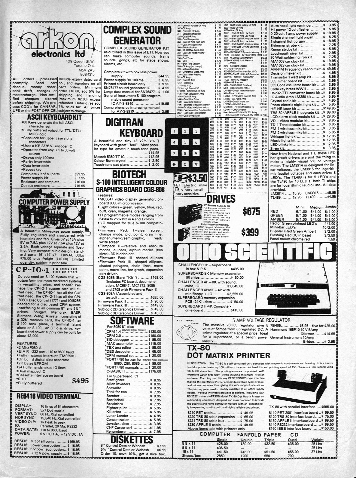
My Superboard was shipped, ungloriously, wrapped in aluminum foil. Manuals were photocopies. It cost about $400 CDN at the time (circa 1979, about $340 USD using the exchange rate at the time) with 4K of RAM on the board – the upgrade for 4K more of 2114 SRAM costing an additional $60 or so (in 1979 … the prices of RAM were quite high then). I built a power supply for mine using a 78H05 5Volt 5Amp regulator as well as a video modulator from a kit in order to use the machine. The advertisement to the right is circa 1981 (from Electronics Today magazine, April 1981) from the place I bought it from, Arkon Electronics on Queen St. in Toronto. The place later sold Apple and is now no longer there. Click on the small image to see the full ad which features pricing of OSI systems as well as other electronics available at the time.
 The Superboard used 2114 RAM chips which were organized as 1Kx4 and so two chips were required for 1K Byte of RAM. The superboard had sixteen sockets for RAM for a total of 8K on board. A year after owing the machine I purchased an additional 8K of 2114 chips and built my own RAM expansion board on a 44-pin edge card from Radio Shack giving me a system total of 16K – at $3.65 per chip (for the slower 450ns chips) 8K of RAM costs $60 in 1980 dollars … RAM memory was expensive at the time.
Aside from the “bare board” Superboard II, these units were also shipped as the packaged Challenger 1P version – the identical board in a nice case with a power supply. The spring 1979 OSI catalog listed the following Superboard and Challenger-I systems (prices in USD):
- Superboard II ($279)
Also called a model 600 board, and new for 1979, this was a complete entry-level system entirely on a single board with keyboard, 8K BASIC-in-ROM, video (24 by 24 characters displayed), and 4K RAM (expandable to 8K). The user needed to supply a 5V/3A power supply and a video monitor for a complete system which includes cassette interface on board. - C1P 4K ($349)
A packaged version of the superboard (with 4K RAM) in a metal case with power supply. - C1P MF ($1259)
The same as above but coupled with a 610 expansion board (with 12K RAM on the 610 board plus the 8K on the superboard for a system total of 20K), floppy controller (part of the 610 board), and a mini-floppy (5.25″) drive in a second box connected via ribbon cable. Shipped with OS-65D 3.0 Operating system.
Other available versions included an inexpensive C1P system with a single-sided mini-floppy and 12K of RAM which ran P-DOS (for “Pico-DOS”) since 12K is not enough RAM to run the full OS-65D which was the standard for all of OSI’s larger Challenger 2 machines.
Hardware
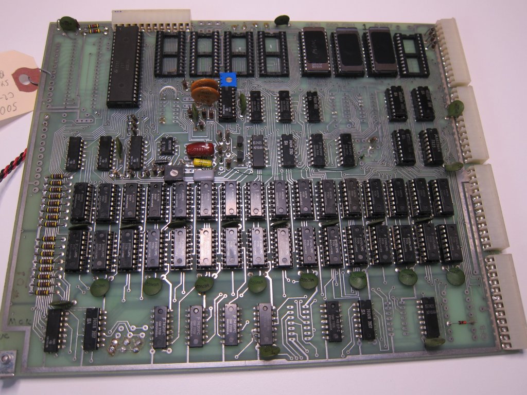
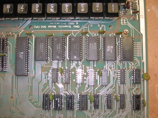
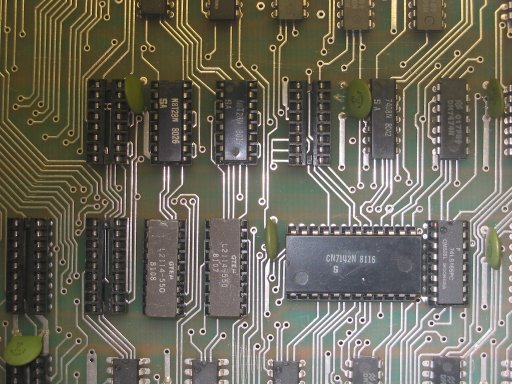
The Superboard and has several notable elements of hardware design, some quite elegant for the time (remember: this was 1978 and so, for example, 2114 1K*4 RAM chips were standard, perhaps even somewhat advanced since a few years before this the 2102 1K*8 chip was used extensively). All of the comments here refer to the revision B board (circa 1978) but apply equally to newer revisions (however chip numbers will change).
 The circuitry was quite simple by today’s standards and most chips were ‘normal’ 74xx series TTL, except for the data bus buffers which were 8T28’s (and difficult to obtain at that). OSI (as well as contemporary Apple) used 8T28 transceiver chips in various circuits. The 8T28 was a quad three-state bidirectional driver. It is unclear why OSI did not use a 74LS245 instead of two 8T28 devices – OSI, for that matter, never used a 20-pin octal device in any of their circuitry choosing, instead, to use two quad devices like the 8T28 as well as 74LS75 quad latches in the keyboard matrix scan circuit.
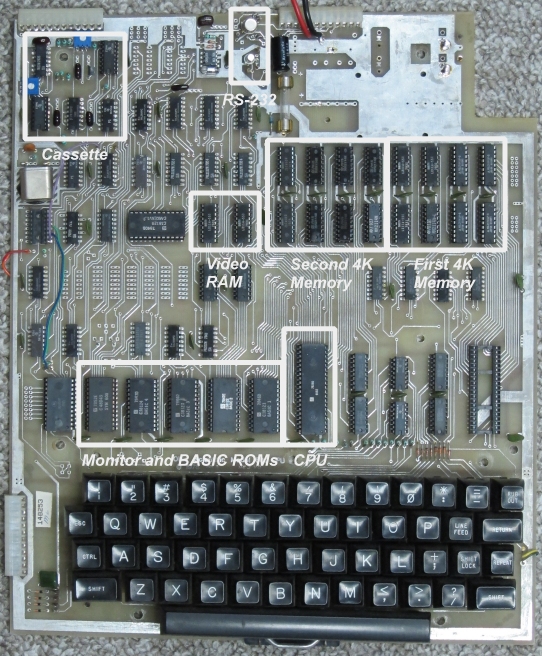
The board contained the keyboard, CPU, ROM, RAM (up to 8K on board), a video section for connection to a monitor or TV via a composite output or an additional RF modulator, and cassette I/O.
Expansion was provided via a 40-pin IC socket. A ribbon-cable jumper allowed this board to connect to a 610 expansion board which also allows connection to an OSI bus (it was rare, though, to expand a C1P system in this way). The 610 board featured RAM (up to 24K more) and a floppy-disk controller. In my case (i.e. since the expansion board probably cost as much as the original machine), I built my own expansion boards in which the OSI expansion connector was connected to several 44-pin card-edge sockets. I had built an I/O port board for the unit as well as a RAM expansion unit (for 16K of total RAM).
The entire board, like other OSI products, was fabricated on simple plated-through, double-sided printed-circuit board. Traces are fairly wide (by today’s standards) making the board both serviceable and easy to repair. You might also note several blank prototyping areas on the board allowing easy modifications as required. In addition, there was an uninstalled RS-232C port which needed a handful of transistors and resistors to implement.
I have included a PDF containing all of the OSI 600 Schematics for a Revision B (circa 1979) board and diagrams for the Ohio Scientific Model 600 Board.
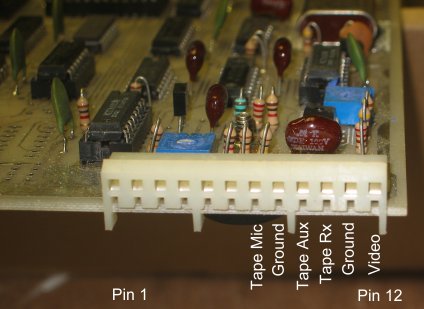
Here are a few photos showing details of the board including pinouts of the I/O connectors …
While my original board was a revision B, the newer revision D boards – functionally similar to the C1P series II – were enhanced to include RAM for colour video and had an installed RS-232 port. These boards feature a connector (J3) for connection of a 4-pole, 3-position switch allowing connection of the on-board serial port to the cassette, a modem, or a printer. This connector must be installed in order for the cassette to operate. Other features of the rev D board include provisions for colour video and a delayed power-on reset where the BREAK key must be pressed for two seconds to effect a reset (fixing what was perhaps the number one complaint of users – an accidental press of the break key to the right of the keyboard caused an immediate reset on the ‘B’ version).
A PDF of the newer Revision D board can be found here: OSIRevD-Sheets.
Video
One of the best selling features of the Superboard was integrated video. The Superboard featured a 24 by 24 character display (yes, only 24 characters across) held in 1K memory mapped from $D000 to $D3FF. It was arranged in memory as 32 x 32 characters however not all are visible. From page 8 of the revision B schematics we can see the video RAM is selected via U55. Signal /WVE (Page 2) selects video RAM into 6502 memory map when A10&A11 are both low.
Video RAM is interleaved between the video scan logic and the processor where it is mapped into the memory area. The 6502 CPU lacks a true DMA mode as it continually outputs an address on lines A0-A15 (the elimination of tri-state drivers on the address lines was done when the chip was designed to reduce chip size and hence cost) however actual data transfer on the bus occurs only when the “phi-2” clock signal is high. This allowed external circuitry to access memory during the ‘off cycle’ when the CPU was not using the bus and this is precisely how OSI implemented video. Of course address lines must be selected by 74LS157 2-to-1 multiplexers to route them to the CPU or the video circuitry depending on the state of the clock.
The address decoder (Page 2, U23) Y6 output ($Dxxx with A12 on U20) selects video on U20. U20 output Y7 then selects video RAM for writing when A10 & A11 low, mapping the RAM to location $D000 to $D3FF. The RAM is mapped to the 6502 CPU only during phase-2 clock, where A0 to A9 on the RAM chips are mapped to 6502 CPU lines. Alternately, when not connected to the CPU, these RAM address lines are connected to clock lines C3 to C7 (five lines = 32 characters) and C11 to C15 (five lines = 32 scan lines on the monitor). Clock lines C8 to C10 selects the line (eight rows scan for each complete character) – these are actually connected to A0 to A2 of the character generator ROM to select the row of the character to use with row 0 the top row, and row 7 the bottom row.
Shift register U42 clocks eight pixels (dots) across from the pattern stored in the character generator at the rate of CLK (the crystal frequency of 3.93216MHz = the dot clock). The RAM location is then incremented (address lines C3-C7) and the next eight pixels are scanned across. 256 clock cycles later, lines C8-C10 increment to point the character generator to the next row. The same memory locations are scanned again and the process is repeated for eight rows completing one line of 32 characters. Address lines C11 to C15 then increment and the next line of characters is scanned. This repeats 32 times for 32 rows of characters.
One-shot U65 generates a horizontal sync pulse at the end of each line (C7, at 15.375KHz) and a vertical sync pulse at the end of each frame (C15, at 60.0 Hz).
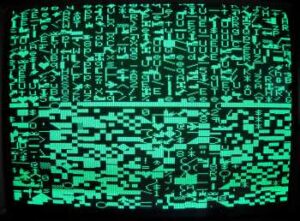
Upon boot-up, a screen full of random characters appears (the random characters corresponding to the contents of RAM when first powered-up). When the BREAK key is pressed (on the latest revision of the Superboard this happens automatically), the screen clears and a boot prompt appears. The video section is essentially independent of the processor and even with no CPU chip installed should display a screen of random characters as seen here.
The C1P video section is almost identical to the (older) 440 video card used in original C2 (500 series) systems. It is, of course, incompatible with the newer 540 video which had twice the video RAM and supported a 64-column display.
Memory:
For simplicity, static RAM was used. At the time (circa 1978), dynamic RAM existed offering a significantly higher density per chip however DRAM, in those days, required three power supplies (+5, +12, and -5V or -9V) as well as requiring periodic refreshing of memory cells – implementing DRAM on a simple computer such as this would require the addition of significant amount of hardware (although OSI did offer a DRAM board, the 530, for larger bus-based C2 systems).
RAM is simple: 74LS138 decoder U23 (Page 2) decodes the 64K address region into 8K blocks, the lowest of those blocks being the on-board RAM. Further decoding is performed by U22 into 1K blocks for each pair of 2114 RAM chips on Page 3.
The four BASIC ROMs are mapped to $A000 through $BFFF in four 2K blocks via 74LS139 1-of-4 decoder U17.
Monitor (SYNMON) ROM must be mapped to the highest 2K of memory ($F800 through $FFFF) since it contains the reset and interrupt vectors. This is accomplished by combining the highest 8K block selected by U23 with A12 via U15 and A11 via U19.
Miscellaneous I/O:
The Polled keyboard is organized as an 8×8 matrix which is scanned by firmware. It consists of a latch and input port selected via U20 (mapped to $DF00 but in reality mapped to a 1K memory block for simplicity).
The ACIA is mapped to $F000 (and $F001) via U17 (likely used since it is the second half of the decoder already used for the BASIC ROMs).
Normally, the ACIA is used for cassette I/O via the Frequency-shift keyer (FSK) transmitter and receiver on page 7. Baud rate generation is provided by U57 which is 300 baud for the standard cassette port – if using the ACIA for an RS-232 serial port (see notes in a section below) it may be increased up to 9600 baud by changing the input on pin 2 to a higher clock frequency in the chain of clock dividers (U30/U59). For example, connecting pin 2 to the CLK clock line yields 9600 baud operation (useful when bypassing the cassette altogether and loading programs from a PC).
Using 2716 (or 2816) ROMs
A popular modification was to upgrade the SYN600 monitor PROM to a third-party one such as CEGMON. CEGMON gave the user line editing abilities with a movable cursor (e.g. the RUBOUT key under CEGMON will backspace properly and have the cursor move to the left which did not happen with the original SYN600 monitor which just showed a backspace as an underscore to the right requiring the user to count the number of characters erased). The BASIC-3 ROM was also often upgraded to fix the infamous “garbage collector” bug which chewed-up memory when arrays of strings were used. Today, a number of collectors must use 2K*8 EPROMs (2716) or EEPROMs (2816), regardless, to replace missing or defective ones on the board. When using replacement ROMs instead of the factory masked 2316 ROMs one must jumper the sockets so that:
- Pin 21 is +5V (this is Vpp for EPROMs and the write-enable pin for EEPROMs – both normally kept at +5V)
- Pin 18 is /CE, the active-low chip enable line
- Pin 20 is /OE, the active-low output enable line
Functionally, both /OE and /CE must be low to enable the chip. If using an EPROM or EEPROM in a masked ROM socket pin 21 will often be connected to the non-inverted phi-2 clock to enable the device only when the clock line is low. I personally like to use 2816 EEPROMs and they resemble the original masked ROMs (plastic package, and without a window) and are easily programmed in a homemade programmer since they do not require high voltages nor a critical pulse width to program – a simple microcontroller could easily be used to rig-up a programmer for these.
The wiring modifications for a revision D board to use 2816 EEPROMs are as follows:
Character Generator ROM: Cut traces currently between pin 18 and +5V and between pin 20 and +5V. Run a wire from each pin (18 and 20) to ground (pin 12 on the ROM).
Monitor ROM: Leave pin 20 (assigned to the /MCS line) alone. Cut the trace from pin 21 to ground (the jumper is below the monitor ROM) and wire it to +5V (this de-selects the write-enable when using 2816 EEPROMs). Cut the trace from pin 18 currently connected to the inverted phi-2 clock and wire it to the non-inverted phi-2 clock (found easily as it connects to the enable pin 14 of the nearby 6850 UART). Note that this change (pin 18 to the non-inverted clock) might not be needed at all! I have tried it without this change (I forgot this one wire) and it worked fine. In theory one should enable the chip only on a low clock though so I cannot guarantee it would always work without this change.
BASIC ROMs: Follow pin 20 from each ROM and cut the traces before they reach the output of the 74LS04 inverters (U16) – two cuts on top and two cuts under the board are required. Run wires from pin 20 of each ROM directly to the outputs from the 74LS138 decoder (U73) – pins 12-15. As well, pin 18 of all four BASIC ROMs are wired together and tied to +5V on the original board – cut this single trace (it can be found below the BASIC-4 socket) and jumper it to ground.
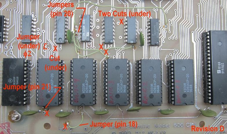 A photo detailing the jumpers for the monitor ROM as well as the four BASIC ROMs for a revision D board is seen to the right. You will notice that my board uses 2816 EEPROMs (pin-compatible with 2716 UV EPROMs) and CEGMON was installed in the monitor ROM socket to upgrade the SYN600 monitor. Wiring for the character generator ROM was accomplished under the board with two jumpers.
For a revision B board the modifications are somewhat different. For the Monitor ROM one could leave pin 20 (assigned to non-inverted phi-2 clock) alone. Ensure pin 21 is connected to +5V to ensure no writes to a 2816 EEPROM can occur. Pin 18 must be cut (it currently connects to the output of an inverter on U18 – pin 4) and must be routed to the non-inverted /MCS signal (same inverter, pin 3) which is active-low. For the BASIC ROMs follow pin 20 from each ROM and cut the traces before they reach the output of the 74LS04 inverters (U16). Run wires from pin 20 of each ROM directly to the outputs from the 74LS139 decoder (U17) – pins 4-7. This is a similar modification to that required with the rev. D board. In addition, pin 18 of these four ROMs is run to +5V on the original board – pin 18 (/CE) must now be jumpered to ground to enable the chips.
RS-232 Connection
For storage and loading of programs originally on cassette tape, MP3 files can be used to store old tape images and load them back into the machine but a better solution (i.e. completely digital and error proof) is to use the RS-232 port to load and store BASIC programs to a PC running a terminal emulator package such as Teraterm or Hyperterminal. This is facilitated by the fact that typing ‘LOAD’ or ‘SAVE’ on the machine simply echoes data going to the video display to the ACIA and accepts data arriving at the ACIA as if it were typed on the keyboard – this is one of the stranger features of an OSI C1P system an reminiscent of old PDP-8 teletype-based systems. For a PDP-8 running FOCAL, for example, the user ‘saves’ programs by listing them to the teletype but first setting the paper-tape punch ON so that received characters are punched to the tape. Similarly, the PDP-8 could not ‘tell’ whether a user was entering a program manually or via a paper-tape being read by the teletype so simply loading a paper-tape into the teletype and setting the punch to ‘read’ mode caused characters to be sent to the PDP-8 and the program to be entered.
So, typing ‘SAVE’ on an OSI C1P system simply routed all text destined for the screen to the serial port as well (ditto for the ‘LOAD’ command). In that respect, simply replacing the FSK demodulator for the cassette tape system with an RS-232 level converter allows the Superboard to load programs from that port. Note that earlier 500-series systems often used an RS-232 serial connection to a console terminal instead of a video display and keyboard – video display was an added board and an added option.
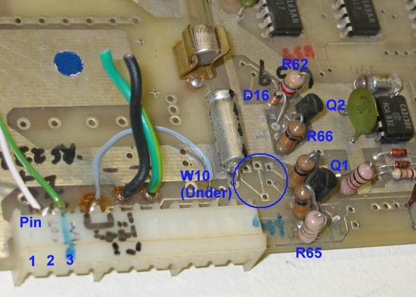
Revision D boards often come with the RS-232 option already installed, all that is required is a switch on J3 allowing the user to select cassette, RS-232, or modem operation. Revision B boards have wiring on the PC board for the RS-232 level converters however these must be installed by the user. A series of jumpers configures the input to the ACIA to come from the cassette tape’s demodulator circuitry or from the RS-232 level converter (useful for connecting, say, a modem or for the output line, a serial printer which I did on my original system). In general, to use the serial port on a revision D board one needs to jumper pins 1 to 9 (to ground the /CTS input allowing the ACIA to transmit), and jumper pins 8 to 10 (for 300 baud operation) or pins 8 to 12 (for 1200 baud operation). Pin 2 is the transmit data output.
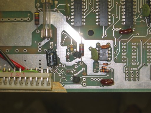
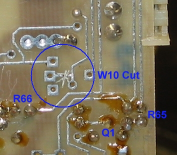
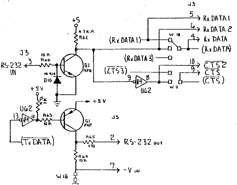
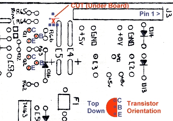
The RS-232 interface (for a revision ‘B’ board) is outlined in the photos below. It requires the addition of two transistors as shown in the schematic – Q1 is a 2N3906 PNP and Q2 a 2N3904 NPN. As well, several resistors and a diode are required to be installed. Follow the circuit diagram, the photograph, and the top-down placement diagram for details. Note the unusual position of the transistors – leads must be bent in an unusual manner (with the base pin out front) in order to be mounted on the board. Otherwise, assembly is not critical.
Connector J3 Wiring (for Cassette Tape operation):
- Jumper J3 Pin 5 to J3 Pin 6
Connector J3 Wiring (for RS-232 operation):
- Jumper J3 Pin 4 to J3 Pin 6
- J3 Pin 2 (RS-232 Out) to DB-9 Pin 2 (Transmit to PC)
- J3 Pin 3 (RS-232 In) to DB-9 Pin 3 (Receive from PC)
- Board Ground to DB-9 Pin 5 (Ground)
After modification, the system should be tested to ensure the cassette operates then the jumper switched and the RS-232 connection tested. On the PC, run a terminal emulator such as Teraterm or Hyperterminal and set it for 300,N,8,1 (300 baud being the normal baud rate of the tape system – this can be changed later). Type ‘SAVE’ on the OSI. Now, anything typed on the OSI keyboard should be echoed to the PC via the serial port, including program listings (this is, of course, how programs are saved to the PC, by capturing incoming data on the terminal emulator program to a text file).
To load a program from the PC into the OSI, type ‘LOAD’ on the OSI keyboard. When something is typed on the PC, it will now be entered into the OSI as if it were typed locally. In this manner program files stored in a text file can be uploaded to the OSI. This method will be considerably more reliable than the use of cassette tapes (or MP3 audio files) – even the original tape system had a high error rate and unless everything was just right, loaded programs frequently had an error or two which required the user to manually correct the offending program line – programs ALWAYS came with a full listing allowing the user to correct minor errors which occurred during loading from tape. The basic unit operates at 300 baud however this can easily be changed (on a D revision board, via J1, and on a B revision board by jumpering a different clock signal into the ACIA).
System Operation and Software
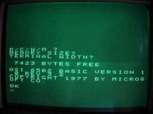 Upon boot-up, the user was presented with a prompt for ‘D/C/W/M ?’ which allowed you to boot from disk, cold boot, warm boot (and preserve memory contents), or enter the monitor to debug machine-code programs. Few systems had disk drives since floppy disk drives alone sold for $650.00 in 1980, let alone the controller! Don’t believe me … look at one of the advertisements above. If an upgraded third-party monitor called “CEGMON” was installed, a similar boot prompt appears on the top of the screen.
Selecting ‘C’ (Cold Start) then pressing RETURN to the “Memory Size?” and “Terminal Width?” prompts completes the boot process directly to BASIC which resides on the board in four 2K ROMs (so BASIC was 8K in length). The amount of actual memory is displayed as well. A system with 8K installed shows 7423 bytes since some is required for zero-page, some for the 6502’s stack, and some for scratch variables for BASIC. A system with 20K displays 19711 bytes – booting from a Disk, for example HEXDOS, will also lower the amount of available memory since the O/S will reside in RAM (and possibly even the BASIC interpreter depending on the O/S used).
Perhaps the most interesting section of circuitry on the system was the video display which used a meager 1K of RAM. Video circuitry in the OSI switched the address and data lines of the video RAM from the 6502’s bus to an internal clock generator composed of binary counters. When a character was retrieved from the video RAM it was converted to a dot pattern by the character generator ROM (U41 in the schematics) which was output as an analog signal representing video levels (black or white). Although the video RAM could store 1024 characters and the actual video RAM was mapped as 32 lines of 32 characters, the actual display was 24 characters across by 24 lines – peripheral characters were not visible and used as a ‘guard band’ to prevent off-screen characters. Later revisions of the OSI board included a socket for a third 2114 video RAM which stored colour information. Further add-on boards (available from third-party manufacturers) even allowed bitmapped graphics with resolutions up to 256 by 256 pixels! (This, incidentally, would require at least 8K of video RAM for a monochrome display where each pixel could only be ‘on’ or ‘off’ … more than most OSI systems were shipped with). RAM, in those days, was a precious commodity and these were the most expensive chips in the machine.
The inclusion of an on-board video generator was a big selling feature of the Superboard-II since some OSI systems using 500 series hardware required an RS-232 ASCII terminal. Back in the late 70’s, these terminals cost more than the machine they were attached to! Many (some older, and some larger 500 series) Challenger-II systems did feature video as well but using a separate video card which, of course, increased the cost of the system. At 24 characters across, an ordinary TV worked quite well for a display and so a common configuration was to use a video modulator allowing the machine to output on channel 3 (this was NTSC, of course).
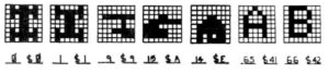
And as a huge bonus the character generator supported ASCII characters as well as a large number of graphics characters for games. Character zero, for example, was a race-car so where you’d normally drop a character 0x41 into a video memory location to make an “A” appear there (e.g. “POKE 53381,65” would make an “A” appear in the upper left corner), a character zero could cause a race-car to appear. Similarly, characters 248 through 255 depicted a tank in one of eight possible orientations 45-degrees apart, as used in the “tank for two” game (below, left). Some gaming graphics were large and required two side-by-side characters including contemporary Star-Wars fighters, Starship Enterprises (Character codes 9 and 10), and ships and submarines. The machine lacked enough memory to allow true bitmapped pixels.
Software was supplied on cassette tape which loaded at 300 baud. You could actually watch the data as it was loaded into the machine which took an average of 3-5 minutes per program. There were a few suppliers of software, one of the most prominent as I recall was ‘Aardvark Software’ which supplied cassettes with a green label. A few examples of BASIC programs written for the Superboard may be found in this zip file: BasicPrograms.
Misc. Modifications
The early eighties were a time of homebrew computers. Unlike the days of the PC, where even an amateur could buy a peripheral card or upgrade and install it, to upgrading a computer in the early eighties required most users to become quite fluent in hardware (and to own a soldering iron). It was common for users to make extensive modifications to their machines.
‘Micro’ magazine (among others) was dedicated to the 6502 and 6809 crowd. Featured articles included the making of a coprocessor board to do complex mathematics (yes, a real Intel math coprocessor attached to an OSI CIIP!), adding I/O to an OSI system, and numerous software articles most using machine code. The magazine covered 6502 systems like the Apple, OSI, and Rockwell AIM-65. Surprisingly, the magazine was not Apple-centric (as this was the most popular 6502 system at the time) – likely because it was a bit of a ‘hardware hacker’ magazine.
OVERCLOCKING was popular even with machines such as these. One of the modifications I made to my original machine was a ‘GT’ option which increased the clock frequency from 1MHz to 2MHz. I found the original documentation on this and scanned it for your amusement:
“GT MODIFICATION FOR 600 BOARD
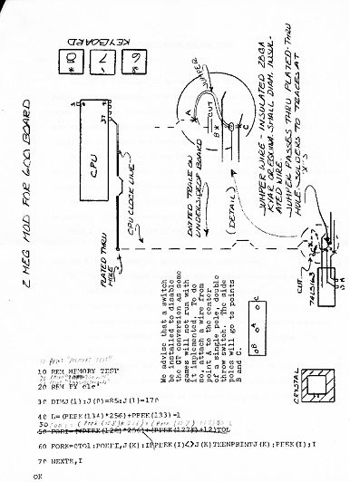 The CIP or Superboard II as delivered by OSI has a primary clock frequency of 3.932l60MHZ. This frequency is a multiple of 60 (the video vertical sync frequency) and also 15,360 (the video horizontal sync frequency). One cycle of this primary frequency corresponds to a single dot, or 1/256th of a horizontal scan line on the monitor.
The clock signal fed to pin 37 of the 6502 is the primary frequency divided by 4, or .98304MHZ. This is within 2% of the nominal lMHZ which most vendors advertise, for 6502 based systems (KIM, SYM, AIM, APPLE, ETC.)
Fortunately for us, a clock frequency of 1.96608 MHZ (approx 2 MHZ) is available in a very convenient spot. With a short length (1″ or so) of small diameter insulated wire, a sharp instrument to cut a trace, and two simple soldered connections, you too, can be running your 600 Board at twice normal speed.”
The instruction sheet goes on to describe in detail how to connect the clock, then it warns you as follows:
“Both the basic proms and the monitor prom have fast enough access to run at the 2MHZ rate. There could be a problem with 2114 memory chips, especially on the CIP because of the enclosure. Chips get a little warmer when you box them up and don t circulate the air. I have one chip in my system that gets flaky after about an hour. I’ll either replace it or put in a fan”
… Some things just haven’t changed over the years: computer types are ALWAYS trying to push their chips past the limit!
Other popular hobbyist modifications to the superboard included homemade RAM expansions and increasing the speed of the cassette system to 600 baud.
Floppy Disks
Up to now, this page has outlined the basic Superboard / Challenger-1P machine. It was possible to add a floppy drive as well however in 1979 – 1980 floppy disks were not all that popular given the extraordinary cost – an 8″ floppy disk drive (the standard in 1980 on all challenger 2 OSI systems) sold for $650 – more than the cost of the superboard and over $2500 in 2026 dollars!. The superboard normally used mini-floppy drives (5-1/4 inch) which were cheaper at $400 but still out of the reach of many hobbyists since adding a floppy still required both memory expansion plus addition of a disk controller like the 610 board or a homebuilt equivalent – adding a floppy drive tripled the cost of a system so many systems used cassette only for program storage.
The rest of this page outlines the use of a floppy disk with the system.
The Floppy Controller (610) Expansion Board
Although a number of hobbyists built their own floppy controller boards (Elektor magazine even featured an article on this in the early 1980s), Superboard and C1P systems from OSI used a 610 expansion board from OSI for floppy-disk based systems. This board contains up to 24K of 2114 RAM on board (48 eighteen pin sockets) as well as a complete floppy controller. With 24K on the board, the system would have the maximum of 32K installed but frequently OSI shipped the 610 with only 12K on board and so the system had a total of 20K – considered adequate for running the OS-65D operating system.
 Calibrating the disk controller on a 610 board
Unlike more modern systems that used a dedicated floppy disc controller chip, OSI built their controller using a simple ACIA chip to handle serial data and PIA to handle control lines for the drive- this is the same approach OSI used in their 470 controller for their challenger-2 machines. This meant incompatibility with any other system but then again floppy-disc systems weren’t all that common in 1979 and even the contemporary Apple-2 used discrete chips to implement their controller.
There are four one-shot pulse generators which must be setup on the 610 board. The numbers given are for a 5.25″ mini-floppy disk (eight inch drives were not normally used with a 610 board, although with minor modification they could be). Remove the floppy disk drive cable from the drive. First, adjust the Tx Clock which will be used to test the Rx circuitry later …
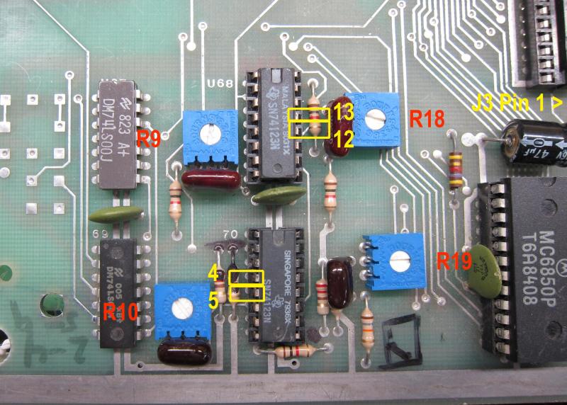
 Put a scope on pin 13 of U68 (74LS123). You should see a series of repeating pulses at 125KHz (ensure it is actually 125kHz as an improperly applied “GT” option with a 2MHz CPU clock could cause this signal to be wrong). Adjust R18 so that each pulse has a positive pulse width of 400ns. This sets the Tx Clock generator which receives a 125KHz square-wave and produces narrow pulses. Now, put a scope on pin 12 of U68 (74LS123). You should see this line high with a series of negative-going pulses at 125KHz. Adjust R18 for a negative pulse width of 400ns. This sets the Tx Data pulse.
Now, adjust the Rx circuitry by injecting the Tx Clock pulses into the received data/clock lines … Place a jumper cable between pin 9 and pin 10 of the floppy output connector on the 610 board (pin 24 is the one nearest the edge of the board and pin 1 the furthest inward). Put a scope on pin 5 of U70 (74LS123). Adjust R10 for a positive pulse width of 1us. This is the Rx Clock. Move the jumper cable between pin 9 and pin 11 of the floppy output connector on the 610 board. Put a scope on pin 4 of U70 (74LS123). Adjust R19 for a negative pulse width of 6us. This is the Rx Data pulse.
If problems are suspected with the 6821 (located at $C0xx), that chip can be tested by removing J3 and executing the following commands in BASIC:
POKE 49153,0 //Selects the Control Port
POKE 49152,1 //Sets PA0 to be an output
POKE 49153,4 //Selects the I/O Port
POKE 49152,1 //Sets line PA0 high (check pin 2 with a logic probe)
POKE 49152,0 //Sets line PA0 low (check pin 2 with a logic probe)
Connecting a Drive
OSI drives provided separate clock and data signals via a built-in circuit called a data separator. Modern drives, which provide combined clock and data on pin 30 of the 34-pin card-edge connector, require an external data separator circuit to work with an OSI system. One interesting article I’ve found regarding the interfacing of a 610 board to an actual drive is from the Aardvark Journal, Feb. 1982 in an article entitled “OSI AND THE SHUGART SA400 BY STANLEY WINDES” which described the changes required to add a standard Shugart SA-400 floppy drive to an OSI system.
The author writes: “The first thing that became apparent upon examining the OSI hardware was that the Data Separator was not on the 610 Board and it was not part of the SA400 electronics either. After much searching and head scratching I concluded that since the OSI system never misses inserting the clock pulse before each data pulse that is written on the disk, the Data Separator would be easy and simple to design. Some of the disk writing systems withhold some of the clock pulses written on the disk. This makes the data separator much more difficult. The data separator I came up with, and found to work very well, is shown in figure 3.”
The figures that accompany the article can be seen here: SA400Disk.
With an external data separator (built according to the article above), an industry standard drive can be used. Input to the separator is from pin 30 of the disk drive and output connects to pins 10 and 11 on J2 of the 610 board. The controller was calibrated by adjusting the potentiometer to give a 6μs pulse (active high) from the Q output of the 74121 (pin 1). A cable was built as follows which connects the original OSI 610 board (connector J3 – pin 24 is the outermost pin near the edge of the board) to the floppy-disk drive 34-pin connector as follows below, noting that many terminals are left unconnected as the original controller was designed for 8″ drives and these functions did not apply to the 5-1/4″ mini-floppy.
| OSI-610 J3 Pin | Function | FDD Connector Pin |
| 1 | Head Load | 2 |
| 3 | HSelect Drive 1 | 10 |
| 5 | Step | 20 |
| 6 | Step Direction | 18 |
| 8 | Write Enable | 24 |
| 9 | Write Data | 22 |
| 10 | Receive Clock | From Data Separator |
| 11 | Receive Data | From Data Separator |
| 12 | Ground | All ODD Pins |
| 13 | Ground | All ODD Pins |
| 17 | Index | 8 |
| 18 | Select Drive 2 | 12 |
| 19 | Write Protect | 28 |
| 20 | To Ground | |
| 23 | Track 00 | 26 |
| 24 | To Ground |
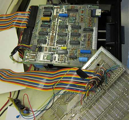 The rear of the OSI 610 board, seen here with a SA400 floppy drive. The multicoloured ribbon cable connects the 34-pin connector on the rear of the floppy drive with the connector protruding from the rear of the 610 board.
Also visible in this shot is the data separator in the lower left. This is the simple two-chip circuit described in the article above built on a small piece of perf board.
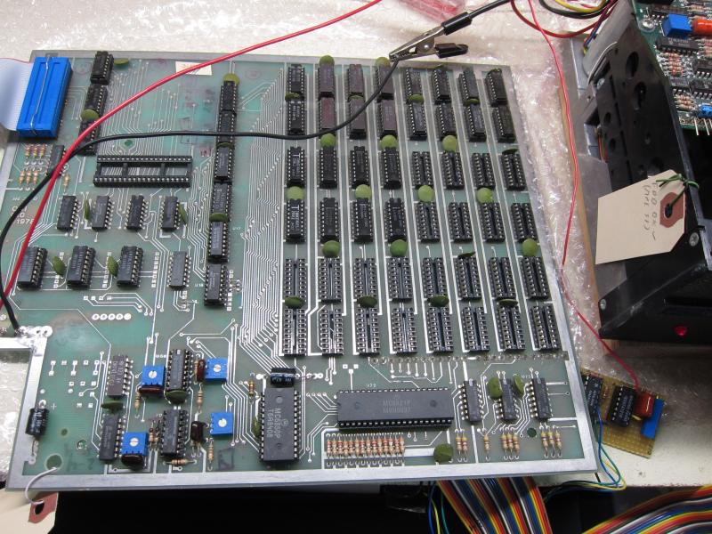
Currently, my 600 board is configured with a 610 memory expansion (24K of 2114 RAM on the 610 board plus the 8K on the C1P for a total of 32K) and using the FDD controller on the board. An external data separator is required. While an OSI MPI-52 drive works with the setup, the Shugart SA-400 requires some patching of the operating system due to a step rate problem as outlined below.
Floppy Disk Drives
Ohio Scientific computers employed unique floppy drives which provided separated data and clock signals. In the beginning (1976), OSI used eight-inch drives made by GSI with a 470 controller board which was originally designed to use such a drive. Later eight-inch drives shipped by OSI, made by Siemens and Shugart, also featured data separators on the actual drive . Such drives use pin 30 as clock (separated) and pin 34 as data whereas ‘industry standard’ drives on many other machines featured a single, combined, output on pin 30 only. These drives also used AC drive motors which ran continually – no motor control was required.
When OSI went from an eight-inch to a 5.25″ drive for their smaller machines like the superboard/challenger 1P they chose to ship drives made by Micro Peripherals (MPI) which also had internal data separators such as the MPI-51. Like their eight-inch predecessors drive spindles also ran continually and OSI made no provision for drive motor control. Note, though, that not all MPI drives feature an internal data separator. Model 52 drives (which are double-sided), for example, feature a connector on the controller board (J5) which is not normally populated – except for an OSI drive where J5 connects to a data separator daughter board. Where the data separator card is not present, pin 3 of J5 should be shorted to pin 5 so that read data appears on pin 30 of the drive connector and so an external data separator circuit would be used.
Diagnostics of the Floppy Disk System
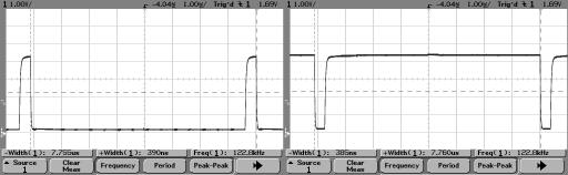
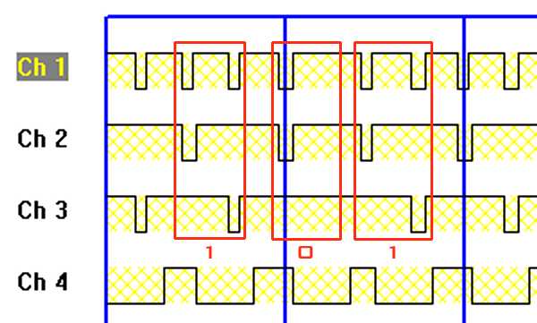
Floppy disks use FM encoding in which a clock pulse consists of a single high-going 400nS pulse every 8μS, an a data bit is encoded as two pulses spaced 4μS apart. This can be seen in the timing diagrams that follows.
 Use of floppy disks with an OSI machine require the addition of a data separator which extracts separate data and clock streams from the incoming data stream from the floppy disk drive. The simple data separator used here consists of a a one-shot and several gates and the operation is illustrated by a analyzer capture of incoming and outgoing signals. The top trace (channel 1) represents data coming from the disk drive and channel 2 the extracted clock stream. For every data bit (whether a logic 0 or a logic 1), a clock pulse (channel 2) is generated at a constant clock rate of 125KHz. Channel 4 shows the low-going pulse from the data separator’s one-shot set for approximately 5.2μS. Each blue line in the capture represents 1μS.
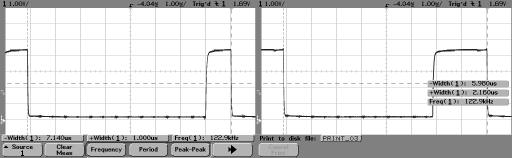
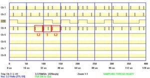
 Operation of the data separator on a stream of data is illustrated in another capture in which each blue line is 8μS apart and three bit cells are outlined from the long stream of data recorded.
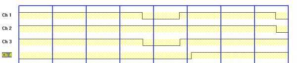
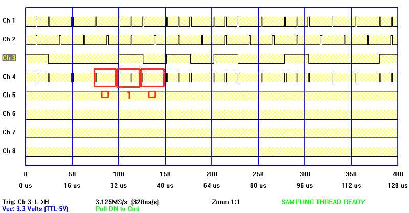
While building a system it was observed that the floppy disk system would boot reliably and reads disks fine (i.e. it can load programs on subsequent tracks on the disk so it is reading beyond track 0) however the write function did not work. A logic analyzer was used to verify the timing and operation of the write logic of the 610 board as follows:
- Channel 1 is pin 8 of the U67 7400 gate which consists of the addition of the clock pulses (channel 2) with data signals from the UART (channel 3). It is the exact format specified for floppy drive write data but is inverted.
- Channel 2 is pin 13 of the U67 7400 gate which is a continuous clock stream consisting of 400nS pulses spaced 8uS apart. This clock stream is generated from the master 125KHz clock on the 610 board whoch triggers a 74123 one-shot (U68) to produce 400ns wide pulses. The pulse width is adjusted by R18.
- Channel 3 is the data stream from the UART at pin 8 of the U69 7404 inverter for data. This verifies the operation of the UART and the inverter.
- Channel 4 is the final data stream to the disk drive, which is simply the inverse of channel 1 (inverted by one sixth of U69) and is used to ensure the output drivers on the 610 board are all functioning.
 The timing of the signals conforms with that outlined in the Shugart SA400 manual – it was verified by the logic analyzer that the write enable goes low as the index goes from low-to-high with the data line consisting of nothing but zero’s (clocks, 8μs apart) until at 1.2ms after the index transition data actually appears on the write data line (a logic 1 appears, followed by a zero, and several more 1’s). When a known good disk is read with the analyzer on the floppy disk lines, a similar pattern appears (i.e. blank clocks on the read data line until 1.2ms after the index pulse goes high) but when a disk formatted on this drive is read in a similar manner, only clocks appear on the read data line. Finally, it seems that the drive is at fault here.
Observing the operation of the actual drive (with the control PCB moved to the side), one can see that it steps erratically. This may well explain the situation since HEXDOS resides on one track so a drive which cannot step properly would still load! I recall reading in an old PEEK journal that HEXDOS can be set for any step rate however the instructions were for HEXDOS 2.3, not my 4.0 version.
Disassembling HEXDOS in memory (remember, it sits on track zero and so loads even if the drive cannot step properly), one finds the stepping routines as follows (with my comments added):
04D2 48     PHA
04D3 9006   BCC $04DB  //If Carry set, step out
04D5 E6D8   INC $D8    //Increment current track # counter
04D7 A9FB   LDA #$FB   //Step out = PB3 low
04D9 D004   BNE $04DF
04DB C6D8   DEC $D8    //Decrement current track # counter
04DD A9FF   LDA #$FF   //Step in = PB3 high
04DF 8D02C0 STA $C002  //Output to PIA
04E2 29F7   AND #$F7   //Isolate bit for PB3 (J3 pin5)
04E4 8D02C0 STA $C002
04E7 0908   ORA #$08
04E9 8D02C0 STA $C002
04EC A203   LDX #$03   //Default step rate - this is the problem
04EE 2091FC JSR $FC91  //Time delay (1.25mS times X)
So, by changing the variable at location $04ED from $03 (5mS step) to $25 (50ms step), the drive can step properly. This is done as follows:
- Boot a copy of HEXDOS 4.0
- Hit BREAK and enter Machine code mode (M)
- Enter address “04ED”, and the data field should display as “03” (the default delay)
- Press “/” to go to data mode, and enter “25”
- Hit Break again and warm start (W) – this preserves memory contents when BASIC boots.
- Load FORMAT from the HEXDOS disk (and it will actually step to that track properly now) and format a new disk
HEXDOS formats all tracks (and you can see it step properly now) then writes itself to track zero of the newly formatted disk. Since it copies itself from memory the new step delay value will be written as well. You now have a patched copy of HEXDOS with a slow step rate that will run on an SA-400 drive. This does not help with booting OS-65D which likely has similar problems with step timing so ultimately, a working MPI drive might be required for that. Furthermore, according to an OSI manual a special version of OS-65D was required for use with a C1P which uses 24-by-24 (440 style) video … this will complicate any attempt to port the O/S from my 8-inch systems to a 5-1/4 inch system.
One final comment of the use of MPI floppy drives with an OSI: apparently the model 51 has a daughterboard (the data separator) but the newer model 52 does not. The following changes must be made to the model 52 drive (as outlined in a very old article by David Livsay):
“To use the newer MPI drives without the separator board you must follow the trace from pin 30 to the 7438 NAND pin 3. Now follow pin 3 of the NAND and you will find it goes two places –
1. Daughterboard connector
2. pin 5 and 9 of the 74LS123
CUT the connection between pin 1 (NAND ) and the 74LS123.”
When I examined a old model 51 board I found that trace is cut (right at pin 1 of the NAND, bottom of the board), whereas on the 52 it is intact.
Hopefully that helps someone else trying to make their floppy system work!
Operating Systems
Ohio Scientific systems normally used the OS-65D operating system which required 20K of RAM. For the superboard/1P a special version was required which supported the 24×24 video resolution (called “440 style” after the original 440 card for the original challenger series) – booting a copy of OS-65D made for a C2 machine will result in a very strange video display. OSI also offered “PicoDOS”for the superboard which was a smaller version of OS-65D specifically for the C1P which, like HEXDOS described below, used the internal BASIC on the board adding only “load” and “save” commands which worked on disk files. (OS-65D loaded BASIC from disk and so could run on a system with no ROMs for BASIC at all which was the case for many larger challenger-2 machines). Unfortunately, PicoDOS could only store eight programs on a disk and all were accessed as a number (1 through 8) so a user would type “LOAD 1” to load the first program on the disk. A popular third-party alternative for many hobbysists was HEXDOS which, like PicoDOS used BASIC from the on-board ROMs however was far more advanced allowing the use of named files (LOAD “FORMAT”). HEXDOS, in general, appears to have been the prime choice for C1P users while those with larger systems (e.g. C4P machines with 64 column video) primarily used OS-65D.
Using the HEXDOS Operating System
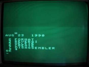 HEXDOS is a simple operating system residing on a single track. It was written by Steven Hendrix in the early 1980’s and was very popular with Superboard users primarily because of the low cost both of the O/S and of the hardware – HEXDOS could run well on a system with only 12K of memory. Unlike OS-65, it does not offer BASIC on disk but rather uses the BASIC residing on the Superboard ROMs – it simply adds LOAD and SAVE functionality (Mind you, disk BASIC was 9 digit while BASIC-in-ROM was only six). When booted (using the “D” option), HexDOS loads then returns immediately to BASIC – the only indication it has loaded being the display of 2.3K fewer bytes free than a cold boot (i.e. 17407 bytes free on a 20K system, for version 4.0 at least). To get a directory of a disk, the “LOAD/” command is used which loads the directory into memory as a program file. Typing LIST displays the actual contents of the disk as seen to the right.
HexDOS supports named files so a user can type LOAD “FORMAT” to load that program . Like contemporary operating systems of the late 70’s, few functions were internal to the operating system and common functions such as formatting a disk or deleting a file required the user to load a program (written in BASIC) to accomplish this.
Internals of the HEXDOS Operating System
It is instructive to examine precisely how HEXDOS works by looking at both the command programs (such as FORMAT) and the disk format itself. We begin by examining the essentials of the FORMAT program, written in BASIC, since this program not only formats tracks but also copies the O/S to the disk using O/S calls. For brevity, only essential code is presented here (not, for example, the required “Are You Sure?” code).
This code generates then writes a blank directory to track one
 160 DATA0,16,0,24,1,2,0,255                  //The data file header region is filled here, 568=char pointer
 170 FORI=566TO573:READT:POKEI,T:NEXT
 180 REM FILE #4 IS NOW DIRECTORY
 190 DATA0,11,1,0,3                           //This is actually the first four bytes of the track 1 directory
 200 FORI=0TO4:READT:PRINT#4,CHR$(T);:NEXT
 210 PRINT#4,A$                               //Date and time header is added to the directory
 220 PRINT#4,MID$("JANFEBMARAPRMAYJUNJULAUGSEPOCTNOVDEC",3*M-2,3);
 230 PRINT#4,D;Y
 235 P=PEEK(566)+256*PEEK(567):T=PEEK(568)-PEEK(566)+2:POKEP,T    //P=4096, and T=21 by inspection here
 236 PRINT#4,CHR$(0);CHR$(T+6);
 240 DATA11,2,0,165,0,0,0
 250 FORI=0TO6:READT:PRINT#4,CHR$(T);:NEXT
 260 SAVE*4                                   //Write buffer to disk (device #4)

This code writes blank tracks 2 through 39
 280 B=PEEK(125)+256*PEEK(126)+10             //B is a pointer to the first array, by inspection B=3698
 290 DIMA(525)                                //Empty array - will fill the track with zeroes
 300 FORI=2TO39:SAVE#I,B:NEXT

This code writes the O/S to track zero from memory
 310 POKE2818,0:SAVE#0,768:POKE2818,11        //2818 is the first byte of the FORMAT program - made invisible here
                                              //then the O/S is copied from memory to track zero
Although we are not privy to the exact format of the disk header, it is observed that the number at location 568, initialized to 1, increments after each character is printed to device #4. After line 200, for example, it has a value of 5. On line 235, T is found to be 21, although the exact function of the POKE in that line is unknown.
The actual format as written to the disk was investigated by examining the data read directly from a working disk. Using the HEXDOS command “LOAD #n,9000” to load 2048 bytes from track “n” to (in this example) location 9000, the memory was then interrogated to see the exact format of bytes on the disk. This was done for several tracks including zero (where the O/S resides) and one (where the directory resides).
Following the format expected by the OSI boot ROM, track zero is special in that it begins immediately with the load address (high, low address) followed by the actual O/S code as follows (with all numbers in decimal since they were dumped using a BASIC program using PEEK and PRINT statements):
03, 00, 09, 32, 182, 03, 21 ...
The vast majority of the FORMAT program above is hence devoted to forming a directory on track 1 which is then updated by HEXDOS as program files are written to the disk. A working directory (from a disk with several programs on it) was read as follows:
87, 01, 27, 11, 01, 00, 03, 72, 69, 88, 68, 79, 83, 13 ...
As expected, the first two bytes are the sync character ($57) and the track number (the third number is once again a mystery). The disk name is seen in the data as “HEXDOS …”. Inspection of that track further reveals directory entries as follows:
... 11, 02, 00, 70, 79, 82, 77, 65, 84 ...
Which spells “FORMAT” which begins on track 2. The actual files on the directory were as follows:
2843
 22597 DOS
FEB 20  5

 2 FORMAT
 3 DELETE
 4 CREATE
 5 DISASSEMBLER
 7 REVERSI
 9 *
Further tracks contains BASIC programs in “core image” format (i.e. tokenized and as it appears in memory) such as track two which contains the actual BASIC “FORMAT” program:
87, 02, 33, 11, 10, 00, 142, 32, 68, 73, 83, ...
Again, the sync character and track number, (and a mysterious third number), followed by “11” to identify the program as a BASIC program, the BASIC token for the line number (two bytes, in binary, “0010”) followed by the BASIC token for a REM statement (142), and the actual text of the remark “DIS …” since the first line of the program was “10 REM DISK FORMATTER FOR HEXDOS”.
Track three contains a program called DELETE for which the first line is “10 FILE DELETE …” as seen in the following dump of track three:
87, 03, 31, 11, 10, 00, 142, 32, 70, 73, 76, 69 ...
All tracks follow a similar pattern.
Disk Format
Although I have a working SA-400 drive I also have an MPI-52 that needs help. In order to assist deciphering what I’m seeing on my scope or logic analyzer I have delved into the actual format on the disk and have outlined it here.
The format of track zero is set by the OSI boot firmware and must be adhered-to by all operating systems (or they won’t be loaded). The actual data begins 1ms after the index hole is detected (the system might well load data immediately, since old versions of OS-65D did not have this delay, however OSI specified it to prevent errors seen with the older versions where the ACIA was initialized as the index hole was detected which might have been in the middle of a data byte preventing the ACIA from synchronizing and resulting in an error-9). After this short delay two bytes specify the load address in memory for the data on this track (with Byte 1 being the high value and Byte 2 the low) – this load address was $0300 for HexDos (3, 0) and $2200 for OS65D. The third byte specified the number of 256 byte pages of data on track zero. It is almost always 8 but in later versions of HEXDOS (4.0) it is 9 with the ninth page being incomplete (only 170-200 bytes) but usable.
The actual track zero holds a guaranteed 2K of data but a quick calculation shows that 199ms of rotation (300rpm = 200ms per track, minus the 1ms delay) at a bit rate of 125KHz (for a 5-1/4″ disk) is 24875 bits or, at 11 bits per byte (which includes one start bit, eight data bits, an even parity bit, and one stop bit per byte on disk) about 2261 bytes which allows for the three initial bytes (load address and number of pages), 2048 data bytes, and 210 “left over” bytes for the incomplete ninth page – not that these last bytes are guaranteed as disk rotation speeds vary a bit.
Tracks 1-39 that follow are formatted according to the OS used. OSI’s standard OS-65D system uses a format where one ms after the index hole sync characters $43 and $57 are found followed by the track number in BCD and a track type code (always $58). Data then follows as sectors which can be variable length: each sector starts with a delay (to separate sectors), a start code ($76), sector number in binary and sector length in binary followed by data.
For HEXDOS, track 1 is the directory which is stored as a BASIC program – the line # of the program is the starting track number on the disk and so the first entry will always be “2”. The last line of the list is “*” to show availability. Tracks 2-39 begin (1ms after the index hole) with a Sync char ($57), the track # in binary, and 2048 bytes of data. Note that there is no sector map in HEXDOS and eight pages of data would appear as consecutive bytes on the track. A program can be multiple tracks, but they must be contiguous.