Prior to (and along with) building the popular Challenger 1P / Superboard machines, Ohio Scientific (OSI) produced several models of computer in the form of multiple boards which plug into a bus. These Challenger 2 models consisted of various configurations from a true single board (using a serial port to communicate with a terminal and with on-board RAM) to a system featuring separate cards for the CPU, RAM, video, and floppy-disk interface. OSI went even further to produce a Challenger 3 series which featured three CPUs (6502, 6800, and Z-80) and even a model with a Winchester (hard) drive: a rarity in any personal computer system in the late 1970’s.
There is also a confusing bit of nomenclature here as OSI often labelled their Challenger 2 systems as “Challenger 4P” and “Challenger 8P” when, in fact, they were really simply “Challenger 2 – 4P” or “- 8P” … this was evident when one looked at the front of a box branded “Challenger 8P” to find the model number “C2-8P”. So, you’ll often see people refer to an “8P” but really, it’s a Challenger 2 – 8P”.
History of OSI Systems
Ohio Scientific (OSI) started business in 1975 and through the late 1970’s and early 1980’s produced a series of 6502-based machines called the “Challenger” series.
The earliest catalog I could locate was the spring 1978 issue. That year, OSI offered several models based on a single-board CPU, the model 500 card. This card featured 8K BASIC-in-ROM, 4K of RAM on board (in the form of thirty-two 2102 memory chips), and a serial port interface. In the most basic offering, the C2-0 Model 500 Board ($298), the user was required to add a power supply and a serial terminal for a basic stand-alone system. The C-28K 500 Superkit ($398) consisted of the basic model 500 CPU board, again with 4K RAM and 8K BASIC-in-ROM, along with a 480 8-slot backplane and 440 video board (with 32 by 32 character display) allowing use with a video monitor instead of a terminal. It was an unpackaged, “open” system in which the user added a power supply and an external ASCII parallel keyboard for a complete system. This system was almost identical to the single-board Superboard II / Challenger 1P in capabilities (although the superboard was more compact and featured a built-in keyboard). Finally the C2-1 500-1 Terminal Add-On ($498) version was basically a simple model 500 CPU board in a case with power supply and standard EIA (RS-232) connectors intended as a “local” computer to run short programs locally.
As well as the systems based on a standalone CPU board, OSI offered more complete cassette- and floppy-based Challenger-II systems. These early machines were housed in blue and black cases (unlike later machines housed in beige ad brown cases).
Cassette-based systems used the model 500 CPU board which featured an ACIA for cassette I/O. Later systems used the 502 CPU which had more memory on board (8K of 2114 chips). The box had a four-slot backplane – the CPU took one, a memory card (if more that 4K or 8K was desired) took another and finally a video card took a third. The final slot could accommodate a model 470 floppy controller if expanded.
The floppy-based systems (e.g. “MF”) used 5-1/4 inch mini-floppy drives. Often a model 505 CPU was used in these systems as it featured an on-board floppy controller saving a slot in the machine (the 505 lacked any on-board memory so a memory card was required, but a floppy system needed more than 8K regardless and so a memory card was always required for such a system).
The largest offerings in the Challenger-II lineup also featured various floppy drive options using standard eight-inch floppy drives. All floppy-based systems were housed in two larger black-and-blue cases, one for the CPU with an 8-slot backplane and separate keyboard and a second case for the floppy drive(s) which had white fronts. Configurations included: A 16K RAM system with a single 8-inch drive (250K) and a serial port (C2-S1S) for $1990, A similar system except with a video card (C2-S1V) listed for $2490, and a 32K RAM system with a dual floppy drive (C2-S2S) for $3090. Note that many systems utilized serial terminals for user interface in the same manner as contemporary mainframe machines did … many larger OSI systems were indeed designed to use terminals (in fact, the front of the 1978 catalog shows a Challenger II system with two eight inch floppy drives and a Hazeltine 1500 terminal in an office setting).
Typical Challenger 2 Systems
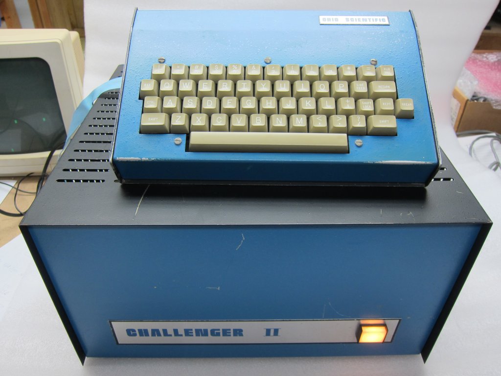
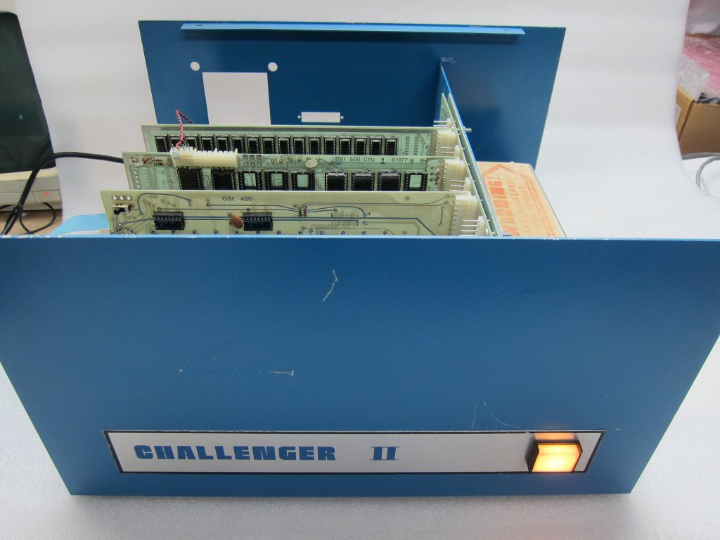
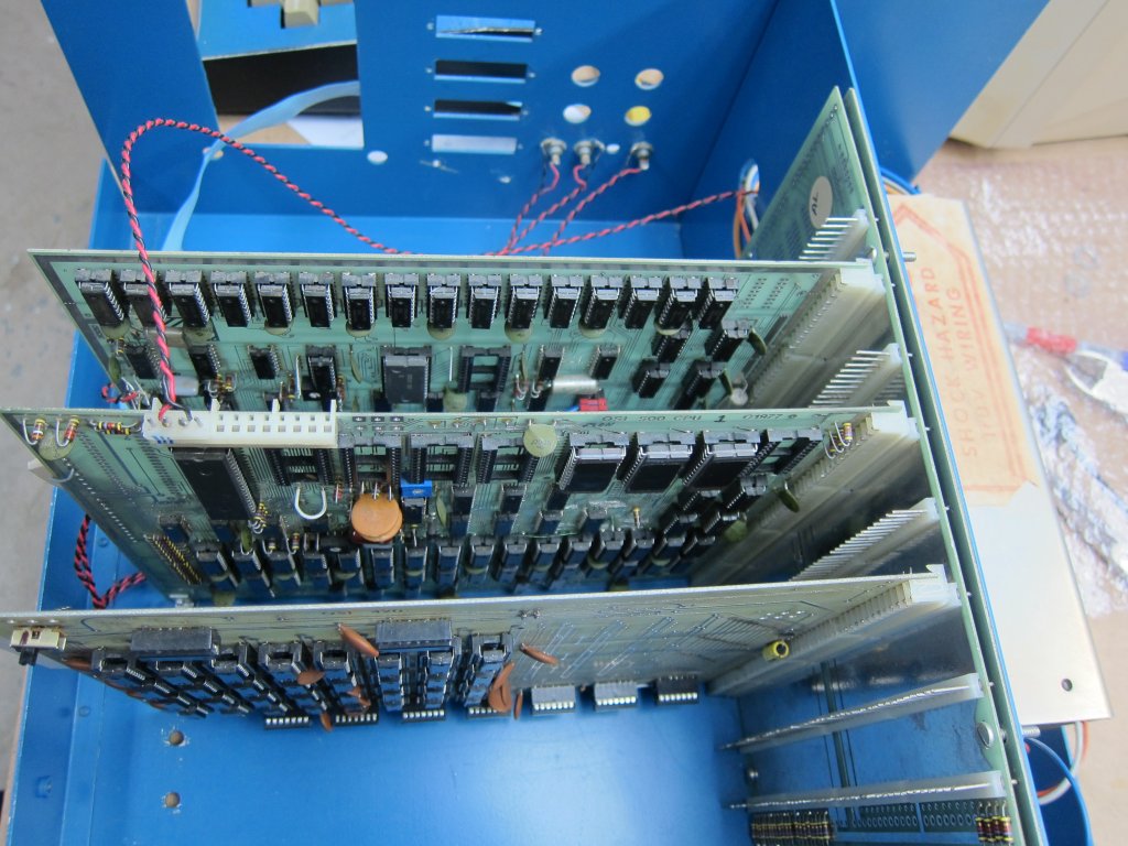
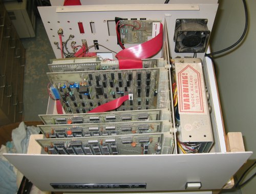
The Ohio Scientific C2-8P was available as a cassette-based system (using the model 500 CPU card) which could be expanded to a full-blown system including eight inch disk drives. This older machine (circa 1977, several years before the popular Superboard II) was packaged in a big blue box featuring separate boards for each function in a large expansion box with an 8-slot backplane allowing expansion. The 8P was intended as a machine for research, educational, or small business use.
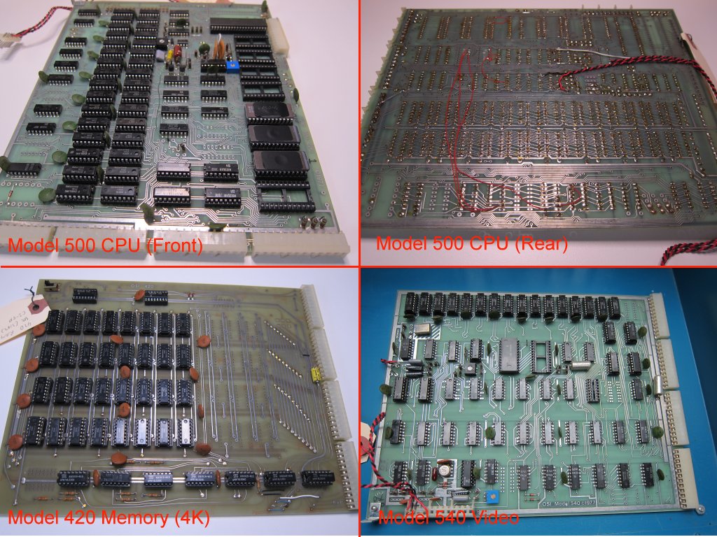
The basic configuration consisted of a 580 Backframe (8 slot), a model 500 CPU (with thirty-two 2102 SRAM chips for a total of 4K of memory on the CPU board), a 540 Video Card (with parallel keyboard connector), and possibly additional cards for memory and I/O expansion (e.g. a model 550 Serial Card for up to sixteen additional 6850 serial ports or a model 420 RAM card for an additional 4K of SRAM using 2102 chips).
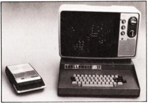
Photos of an early (1977) Challenger C2-8P System
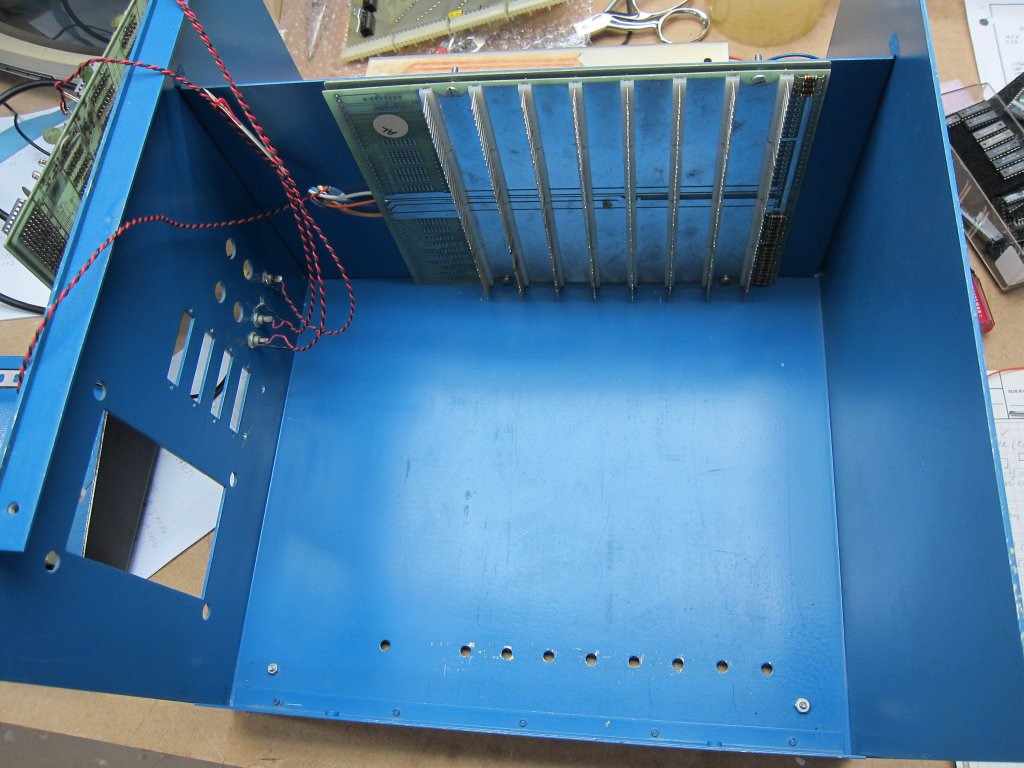
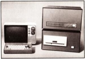
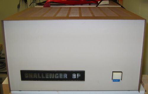
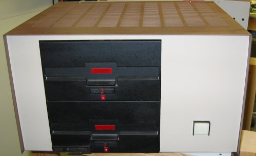
Newer machines were packaged in tan and brown cases. This Challenger 2 – 8P Dual floppy machine is circa 1979. It has a 505 CPU, 540 video card, and three 16K memory boards – five of the eight slots on the backframe are occupied. The 505 CPU has a built-in floppy controller but no memory – that is provided by the three memory cards totaling 48K. The 540 video card has 2K of video memory on board and so can produce 64-character lines. The video card also contains the interface for the keyboard (which was normal for OSI since systems with a video card also need a keyboard … the other option was to use a serial port for the console).
The system features two eight-inch drives (Siemens FDD 100-8 drives) in a box the same size as the CPU and connected via a large (50 pin) ribbon cable. When booted, the screen prompts “H/D/M ?” … unlike the single-board system or cassette-based systems this one does not have BASIC-in-ROM on the CPU board (hence the lack of the ‘C’ cold-start option). BASIC is run from the disk.
Photos of a newer (circa 1979) Challenger-II Dual Floppy (DF) system:
CPU Boards (Hardware)
Challenger 2 systems were shipped with a variety of CPU boards which evolved over time from a generic board (shipped with all systems) to boards which were specific to cassette- or disk-based systems.
Model 500 CPU Board:
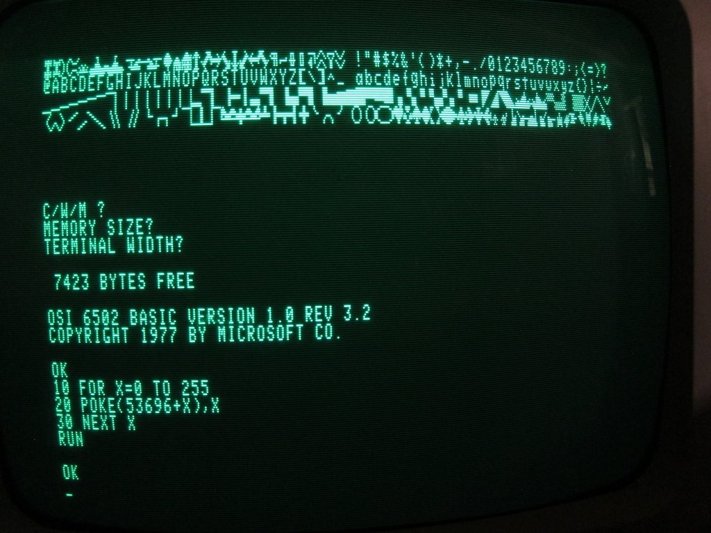
The oldest board (circa 1977) is the model 500 CPU. It was generic and used for serial or video console systems, both cassette and disk based. This CPU features thirty-two 2102 1K*1 SRAM chips on board for a total of 4K of RAM. As shipped with early BASIC-in-ROM systems, the user was presented with a “C/W/M?” prompt reset. It could be used as standalone single-board computer (using the serial port as a console with an ASCII terminal).
Interestingly, the model 500 CPU board lacks a quartz crystal for a clock: instead, two 74LS123 one-shot chip is used to generate a fast clock (about 1MHz) for normal operation and a low-speed clock (about 500kHz) for wait states when accessing slow memory devices.
Systems using the 500 CPU could be expanded to include a floppy disk by adding a 470 card onto the bus, and video using a 540 video card. Addition of any card, of course, requires a backplane (either 4 or 8 slot depending on the model) and a change in the monitor firmware to support video or disk.
This board had four sockets for 2K masked ROMs to hold BASIC as well as three sockets for 1702 (256 byte) EPROMs for bootstraps. These obsolete chips required +5V and -9V to operate and were likely used as they were the same chips employed in the older 400 CPU board. This code was for a monitor, essentially what we would nowadays call a BIOS, and all communications with the user went through routines in it. The simplest configuration of the 500 was as a single-board machine with the 65A ROM which utilized the on-board serial port for user interface. BASIC in ROM will also, then, use the serial port for all commands and program entry when the 65A ROM was installed.
Another available ROM was the 65V which expanded the system to include video and a keyboard via an additional 440 video board (which featured 32 by 32 video displayed as 24 lines of 24 columns). Later video boards featured more lines and columns.
The desired ROM was installed into socket A6 and mapped to 0xFF00-0xFFFF. A switch could be installed allowing selection serial or video by selecting one PROM or another during boot. Regardless of the system (serial or video), on reset, the console will display “C/W/M ?”: “M” selects the machine-code monitor while “C” is a cold start to BASIC and “W” a warm start to BASIC (which retains the program).
Of course, if only a monitor ROM is installed, but not BASIC in ROM, BASIC must then be loaded by papertape (for the serial version) or cassette tape (for the video version). At least 12K or RAM would be required then since BASIC must reside in RAM.
Cassette storage in either case (serial or video) was an option that required an additional board, a 430B, which featured an ACIA and associated analog circuitry.
As well as serial and video options, a floppy-disk boot PROM, the 65F, was available.
An updated 500B board dispensed with the three 1702 monitor ROM sockets replacing them with a single 2K socket. Several versions of the monitor were held on the same ROM with the desired version (serial, video, or floppy) mapped into the upper 256 bytes using a complex scheme involving a 74148 priority encoder chip. Solder pads on the board allowed the selection of monitor.
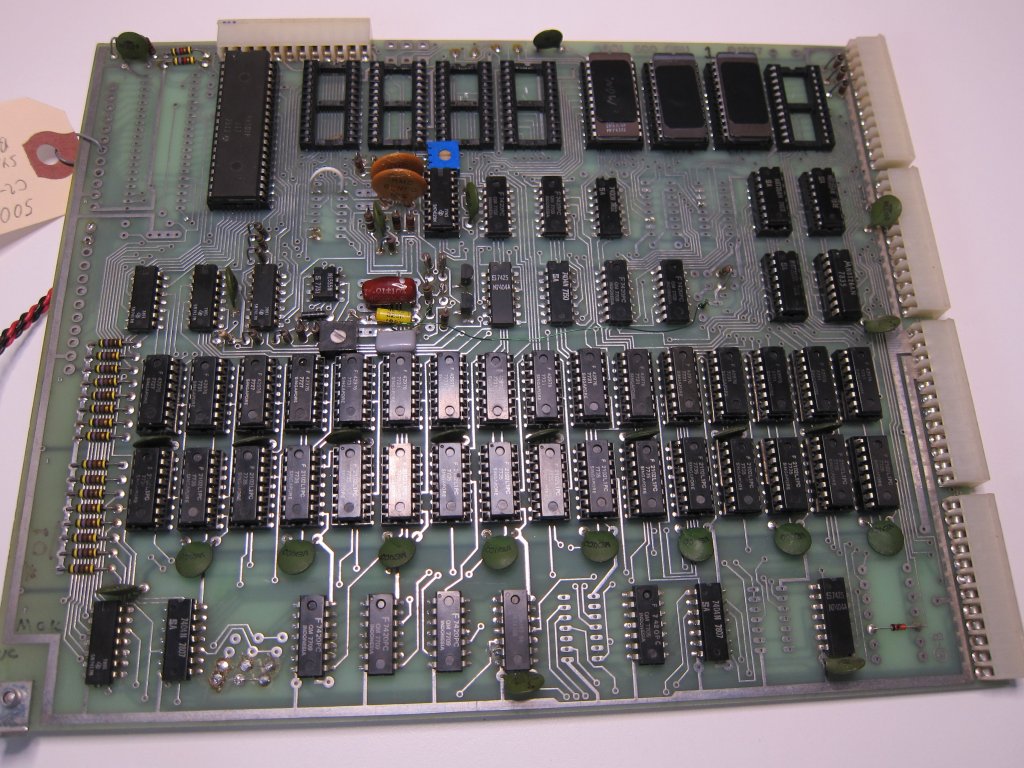
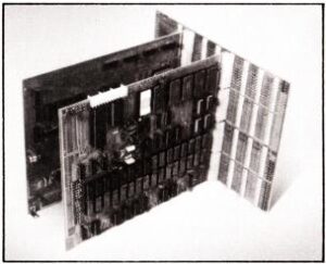
The model 500 CPU card is seen here. The CPU is the large chip near the top left, and the empty sockets next to it are for the original monitor ROMs (on obsolete 1702A EPROMs). The three EPROMs to the upper right contain a new monitor (on a 2K EPROM) and BASIC-in-ROM on two 4K EPROMs. In some systems (often upgraded ones), none of these ROMs are installed on the CPU card at all as they can be put into a (newer) memory card on the bus which supports 2K devices such as the model 538 (available only years after the model 500 was produced). Also visible are the thirty-two 2102 memory chips at the bottom of the board – totaling a whopping 4K!
More information on the 500 CPU and modifications which can be made to it may be found at the bottom of this page.
Model 502 CPU Board:
This board was designed specifically for cassette-based systems. Like the 500B it had five ROM sockets (four for BASIC plus a single 2K monitor ROM which mapped 256-byte segments into the memory space via a priority encoder). It used updated 2114 RAM chips (instead of 2102’s) and so had 8K on board. The board also had fewer TTL logic chips since a multitude of decoders for the older memory chips were not required now. A 300-baud cassette interface (ACIA and associated analog circuitry) was integrated. The C2-4P used this board.
The newer 502 CPU has a similar oscillator but often derives its clock from the 540 video card via the bus (jumper selectable) – be careful when diagnosing this board as you might need a video card in the system just to get the clock.
Model 505 CPU Board:
Used in most floppy disk systems, this board has no RAM on board however it did contain a serial port as well as a full floppy disk controller (using a 6850 ACIA, a 6821 PIA, and associated circuitry). It featured three ROM sockets for the older 1702 monitor chips (often unused solder pads and not even socketed) as well as, more commonly, a single 2K ROM socket with a selectable monitor. BASIC was loaded strictly from disk into RAM so no sockets were provided for BASIC ROMs. Combined with a high capacity memory card for a compact floppy-disk machine (e.g. C2-4P MF).
Model 510 CPU Board:
This board sported three CPUs (6520, Z80, and 6800) and was used in the challenger III line. Coupled with a large amount of RAM often three or four individual boards) it allowed a challenger to run CP/M (on the Z80) in addition of the OSI 65D (on the 6502).
Diagnosing/Modifying a model 500 CPU card:
The model 500 board was available as a kit and so a relatively complete description of the board as well as basic diagnostics may be found to assist in repair. You will need the schematics, regardless, which are also part of the assembly manual to determine how the decoding circuitry works. These can be found at OSI WEB and at Mark’s Ohio Scientific Archive along with many other manuals.
Check the clock first at the 6502 processor on pin 37. It should be around 1MHz. Next, remove the CPU chip and check each section of the 7417 buffers which drive the address lines from the CPU into all other on- and off-board circuitry. This requires a painstaking check of all sixteen elements.
Configure the on-board RAM to start at 0x0000 via the jumpers between F2 and F3 on the bottom left of the card. All four upper address lines (A15 to A12) should be set to “inverted”. At least eight 2102 memory chips are required to give the minimum 1K memory required.
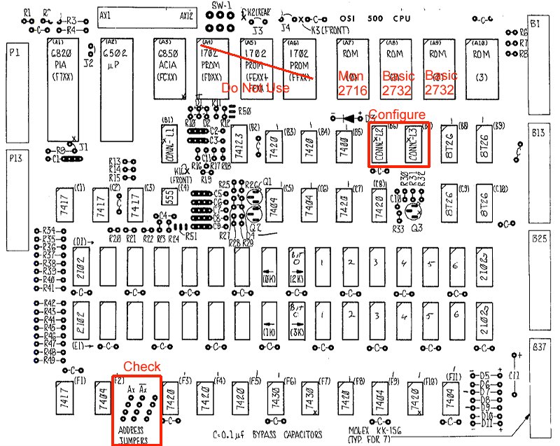
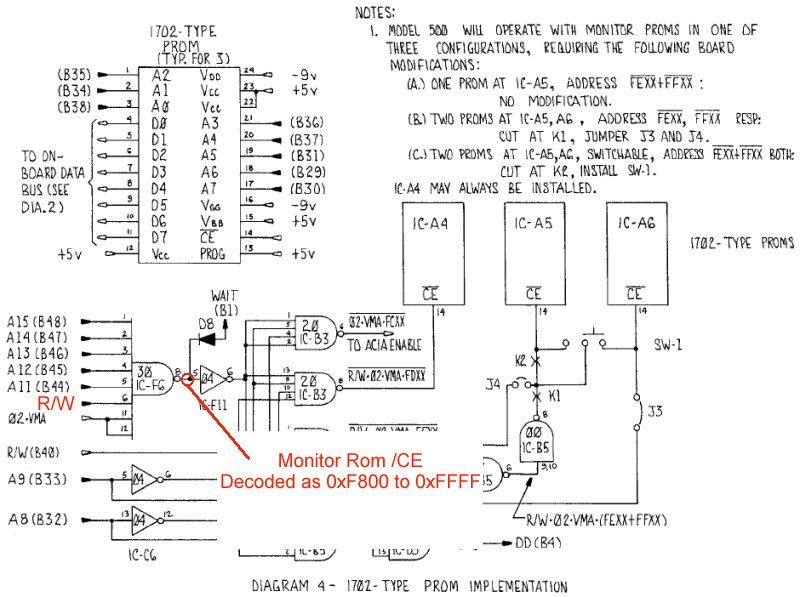
If the ROM monitor exists, you might be lucky that it is the correct one however there were several available (they are different for video and serial systems, as well as those using floppy disks) and so you might need a specific monitor. If you don’t have one, it is difficult to obtain the 1702A EPROMS OSI used on this early board and even more difficult to find a programmer. The easiest solution is to put the monitor on a 2K EPROM either on an external memory card (which takes 2K devices and can map one into the upper memory area), or to install it on the 500 board itself in the first socket usually reserved for BASIC. That socket must hence be mapped to 0xF800 to 0xFFFF. A simple solution is to take IC-F6 (a 74LS30 eight-input NAND gate) and reconfigure it as a decoder. This decoder, used to decode the block used by the old 1702A monitor sockets, is non longer required if using a 2K device. Simply cut the trace which connects A10 to pin 6 and jumper R/W to pin 6. Now connect pin 8 (the output of the decoder gate) to pin 20 (chip enable) on the monitor ROM. Since those sockets are already designed for 2K devices, jumper them for use with a 2716 (which takes care of the other required signals) and the monitor will be mapped to the correct location.
Mapped to 0xF800 to 0xFFFF, there are a number of options for the monitor however only a 256 byte block is required for a minimal system. With a full 2K, the complete SYNMON can be burned to the ROM so that in the future, one could swap memory locations for a disk-based system (inspect the hex file with an editor and you’ll find the “H/D/M” boot code in there as well). This file ( cwmhighhex ) contains the complete firmware for the 2K monitor ROM as used here (for a video-based system with a 540 card installed, as well as with support for BASIC-in ROM) – other variations can be found on the web including the 256-byte minimal version found on the original 1702A ROMs as well as serial versions.
 Unfortunately this causes two problems: First, the UART which was mapped on the original model 500 CPU at 0xFC00 (right in the middle of the 2K monitor EPROM we are to install). According to the manual, it was done this way so the port can act as the console in a system without a video card (i.e. a serial-only system). If your system has video, the port is superfluous and the 6850 can be removed, and if a serial system is desired, more logic will be required to map the UART back into the system at the required location.
For cassette operation that on-board 6850 serial port can be relocated to F000 to F001 (the “normal” location for the cassette port on a newer system), or an additional serial port board (like a 550) can be added to the backplane.
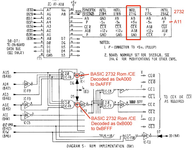
The second problem is that you won’t have four sockets to hold BASIC in ROM. This problem is also easy to solve by burning BASIC ROMs 1 and 2 onto a single 4K 2732 and ROMs 3 and 4 to a second 2732. Two of the remaining three sockets on the board can now be configured for the 2732 devices (mainly just by jumpering A11 to pin 21 of those sockets) and using IC-F8 (74LS20 quad-input NAND) outputs to select the chip enables for those two new ROMs. IC-F8 pin 8 decodes addresses 0xA000 to 0xAFFF for BASIC 1/2 and pin 6 decodes 0xB000 to 0xBFFF for BASIC 3/4 … both are 4K blocks.
Diagnosing/Repairing a Model 540 Video Card
In many systems the video card develops faults which will prevent the system from running. Almost all C2 models employ a model 540 card, either A or B revision. These cards have 2K of video RAM and can display 64-column video (by 32 lines). Here’s a quick guide to diagnosing and repairing such a card:
First determine if your card is a revision A or revision B and obtain schematics for it. The “A” board is a basic black&white board which also contains a cassette interface which translates serial data from an external ACIA (e.g. on a CPU card) to the FSK standard used by the Kansas City Standard tape format. The “B” board dispenses with the cassette interface however features colour, adding 1K of RAM to accommodate it which was configured as 2K*4bits (16 colours).
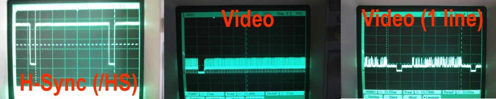
It is easiest to work on the card when it is removed from the system – this will allow 90% of all debugging to be done (all but the interface between the video RAM and the system bus). A working video card will produce a screen of random characters when powered-on, even when removed from the bus. Remove the card and apply 5V power (about 2A) from an external power supply. Connect a composite monitor to the output of the card (pin 7 of J1 is black&white composite, pin 5 is colour composite, and pin 6 is ground). If the video clocking section and character generation logic is working you will see a screen full of characters. If not, the display is often blank possibly with an odd horizontal line so it is time for diagnostics …
Using an oscilloscope (which is pretty much required when doing board-level repairs like this), check for sync signals: /HS (horizontal) should be an asymmetrical square wave mostly high with a thin low-going pulse at 15.7kHz while /VS (vertical) should be a similar waveform but at around 60Hz. If these signals fail to appear, check the 74123 one-shots which generate the thin low-going pulses (these often fail and are socketed accordingly) and ensure these chips are fed with a square wave of the same frequency – These are U4A and U4B on the revision B board. Those square waves are derived from the 3.58MHz crystal via a divider chain of binary counters so check there if the input signals to the one-shots are not present.
Once you know the sync signals are good, check the 7403 gate used to combine and invert these two signals which the pass through a potentiometer and are combined with the video signal via a network of resistors (the 7403 is a quad 2-input open-collector NAND). Careful since black&white and colour boards have some subtle wiring changes and so a potentiometer or several resistors might not be there at all on the colour board.
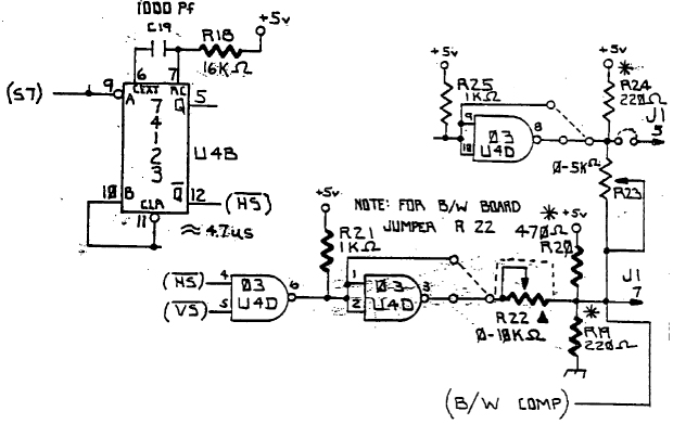
The black&white composite signal then appears on pin 7 of J1 on the board (with pin 6 being ground). On a colour board the output appears on pin 5 via a driver transistor and another potentiometer that sets the output level.
The usual suspects for faults include the 74123 one-shots and the 7403 gate. Of course it is impossible to predict all possible faults – on one board I found a bad potentiometer (R23) which allowed sync signals to be produced but prevented video from appearing … as I mentioned, an oscilloscope is invaluable here.