UNDER CONSTRUCTION
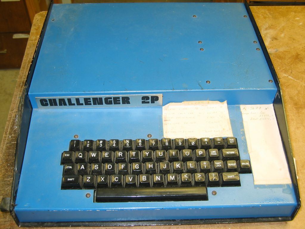
The Challenger 2-4P, introduced in 1977, was the smallest of the challenger 2 series machines which were nicely packaged in metal enclosures with built-in power supplies. This machine was the precursor to the popular Superboard II (the challenger 1P) introduced in late 1978 with the Superboard selling for half the price of a C2-4P system – although the C2-4P had higher resolution video (up to 64 x 32 characters) and was more expandable using an available set of 400- and 500-series boards.
Consisting of at least two boards which plugged into a four-slot backplane, this machine was sold as a BASIC-in-ROM machine with 4K or 8K of RAM and using video output. It could be expanded to include more RAM as well as floppy disc storage.
The Basic System and CPU
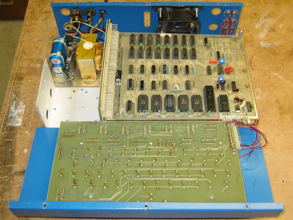
This Challenger 2 is one of the earliest – the serial number engraved on the plate is “Factory Demo” – and so it uses some very early boards from Ohio Scientific Inc (OSI). This machine is based around a model 500 CPU which is plugged into a 4 slot backplane. The 500 could operate either as a standalone machine (with a built-in serial port connected to a terminal such as an ASR-33 Teletype) or, as in this machine, connected to a backplane to communicate with 400- or 500- series boards such as video, memory, and interface cards.
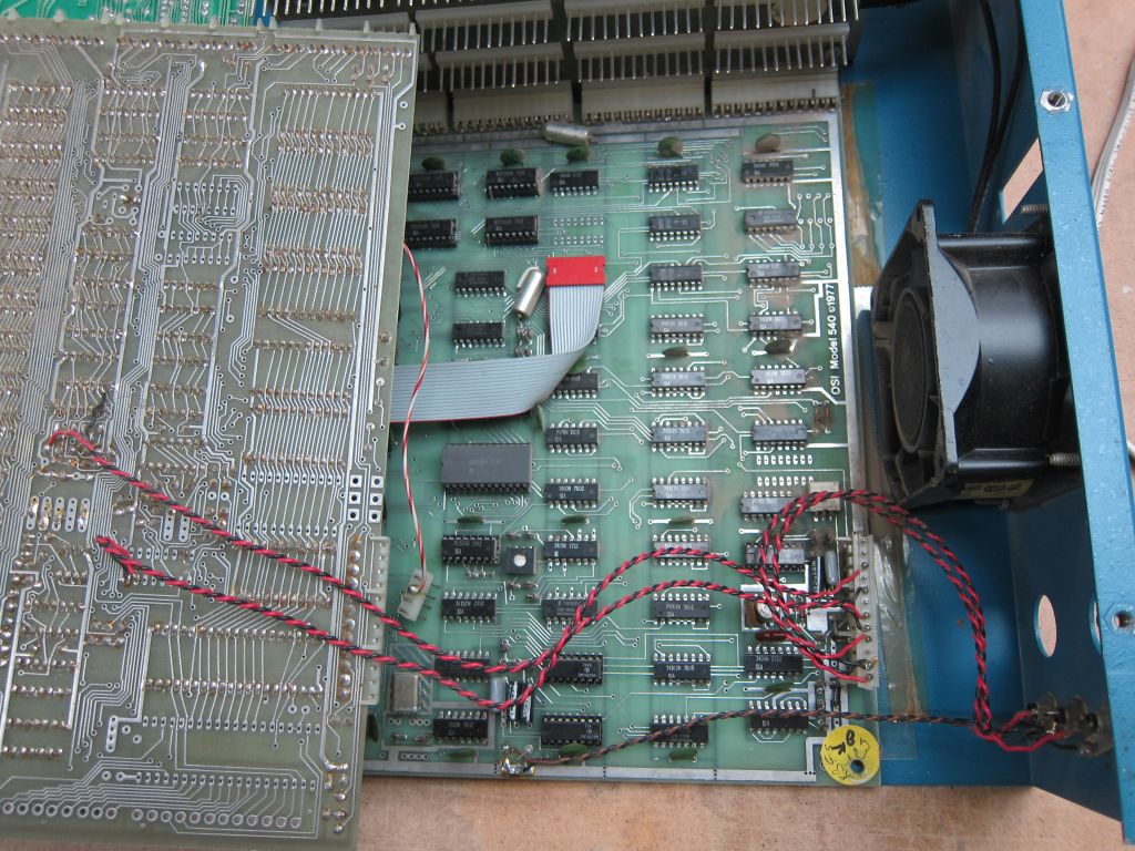
This early model of the CPU board (pre- any revision code) features 4K of 2102 RAM on board. The system has an additional memory card providing 4K for a total of 8K of RAM which was normal for a cassette-based system. Later C2-4P machines used the 502 CPU board which featured 8K of 2114 RAM. The 4P machine is a keyboard machine in which an external keyboard is interfaced via the video card and although the unit has a 540 video card (which normally had connector for a polled matrix keyboard). This unit is so old it uses a non-OSI Keytronic keyboard right from the factory. The keyboard connects to the 540 video card via a small A-10 breakout PCB. The keyboard only supports upper-case characters (see more on this below).
While the keyboard port on a 540 video card provides for interfacing a polled keyboard (which consisting of a latch and input gate – the keyboard connector brings A0 and A1 as well as R/W to the keyboard), this machine uses a parallel ASCII keyboard. Unlike the older 440 video card that has two simple 74125 three-state buffers as an input port which can be interrogated by the CPU at address $DF01, the ASCII keyboard here is connected directly to the two 8T26 buffers for the (polled) keyboard used, effectively, here as an input port to directly read the keyboard . Since the 8T26 buffers respond to all addresses over a 1K block starting at $DF00, a read to $DF01 will route data from the keyboard inputs to the data bus so it can be read. This provided backwards compatibility to read an ASCII keyboard without additional hardware yet still allow use of a polled keyboard. Of course the ROM must support the specific keyboard in use (as outlined below). The keyboard is wired to the 8T26 buffers such that the low seven bits (pins 1-7 on the 540 board connector D9) are data and the highest bit (pin 9) is the strobe and so firmware must poll the strobe line as there is no interrupt.
Two odd points about the keyboard interface here: One, that pin 1 of both 8T26 buffers for the keyboard are bent upwards and so unconnected when in the socket. This means the 8T26’s can function only as a read-only port (logical as this is all that is required when an ASCII keyboard is used) and Two, the A-10 board has an odd non-functional switch installed. Originally it was thought the switch selected the polarity of the strobe however it actually shorts pin 11 (/A1 on the keyboard connector) to ground which effectively shorts the output of a 7404 inverter (IC-D11 pin 10) to ground. Since this line is used only for the keyboard it changes nothing when the switch is flipped.
In addition to the CPU and Video cards, this unit also has an additional memory board, a 420, holding 4K of 2012 memory chips. This was the oldest memory board OSI offered and could be configured for an 8-bit data bus (as used here) or a 12-bit bus when used with a different CPU board using an LSI PDP-8 processor. Newer boards used higher capacity chips (beginning with the 2114 1Kx4).
This machine used cassette audio tape for storage (Kansas City standard at 300 baud) with the analog modulator and demodulator circuitry on the 540 video card. Twisted pairs of wires brought serial data from the CPU card to the video card and from the video card to connectors on the rear of the system. Given the limited memory this early machine would not have been suitable for use with a floppy disk and with only four slots, a memory card with enough capacity would not have been available at the time. As such, floppy disks were available only on larger 8-slot machines (in 1977, at least) like those outlined here. Later (1979) 4P models used a 505 CPU (which had an on-board disk controller but no on-board memory) plus a larger memory card such as the 527 board (which had 24K of 2114 RAM and wasn’t available until mid-1978) for a floppy disk-based system.
ROMs
Like modern PCs that have a BIOS, OSI machines had boot ROMs. Normally, a CPU had either a boot ROM (to start BASIC in ROM or boot from a floppy) or a machine-code monitor, or both. This particular machine has a boot ROM which presents the user with ‘C/W/M ?’ where C or W enter BASIC and M the 65V monitor. The ROM employed is different depending on (a) if the system uses a serial console or a video monitor & keyboard and if it does use a keyboard (b) the type of keyboard (either ASCII in which the keyboard produces a byte representing the key pressed and a strobe or polled where the main CPU scans the keyboard matrix).
This unit has two 256-byte type 1702 ROMS as follows:
ROM A5 at 0xFE00 is the OS65V Monitor
ROM A6 at 0xFF00 is the boot ROM (displays C/W/M, contains IN,OUT,LOAD,SAVE routines for ACIA)
The monitor ROM at $FE00 (labelled “65VP”) and boot ROM at $FF00 (labelled”500V_ 7.3″) appear to be very similar, but not exactly, like those for an older system supporting a 440 video card (on Mark’s OSI site, called “OSI440-65V-ACIA” and a two ROM set).
Differences in the $FF00 ROM include the line start offset of 64 bytes (instead of 100 in the 440 ROM at $FFE0), a line length of 64 characters (instead of 24 in the 440 ROM at $FFE1) and of course the size of the video RAM set to 2K (instead of 1K at $FFE2). Differences in the $FFE0 Monitor ROM include the end page for screen blanking of $D8 (instead of $D4 in the 440 ROM at $FE0C) since the 540 screen is larger.
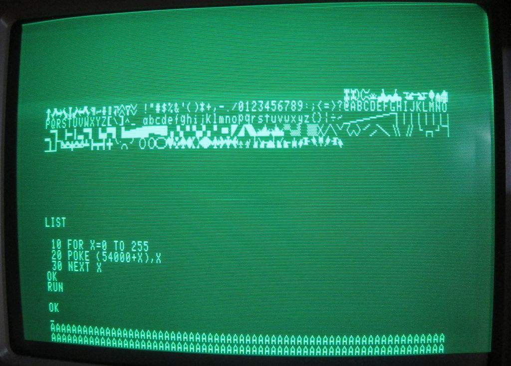
I have included a text file here with the contents of both ROMs which was dumped to a PC via the serial port using a BASIC program as I am not even sure my EPROM programmer supports 1702 devices. The program PEEKs locations 65024 to 65535 and prints the value to the screen – SAVE is executed first so all PRINTs echo to the UART (at 300 baud, mind you, as this is the default speed for tape usage). A 1488 driver was added using jumper clips so that data from the UART was transmitted as RS-232C to the PC.
Inspecting the ASM listing, the boot ROM supports a UART at $FC00 (which the 500 CPU has but is used for tape storage in this system) and an ASCII keyboard at $DF01. Similarly the 65V monitor ROM supports an older S1883 UART (originally used on the 430 board) as a console (at least it resets it, if it were present at all), a 6850 UART at $FCxx for tape I/O (e.g. using the “L” command), and an ASCII keyboard at $DF01.
The 65V Monitor ROM could be used alone in the CPU at $FF00 as it handles the reset vectors but in that case it would boot directly to the 65V monitor (with address and data displayed in the upper left corner of the screen) and there would be no C/W/M prompt nor support for BASIC-in-ROM. The 500 CPU actually has provisions to address a single PROM as both $FExx and $FFxx simultaneously. In the case of this machine, though, separate boot and Monitor ROMs were installed.
When restoring a machine like this, it might become necessary to retrofit the board to accept a standard 2716 2K ROM – this modification is outlined on another page on this site.
As an aside, the SYN600 ROM on a Superboard/C1P contains boot code (256 bytes) and an OS65V monitor among other code (including a floppy bootstrap) in a single 2K chip. The ACIA is located at $F000 on a Superboard.
Totally unrelated comment: while inspecting the code in the ROM which handles the ASCII keyboard I noticed that the OSI machine will hang if the strobe stays low. The code waits for the strobe to end before continuing as follows:
$FFCB: LDA $DF01
BPL $FFCB
So this is one more strange failure mode that is possible if the keyboard produced an unexpected signal.
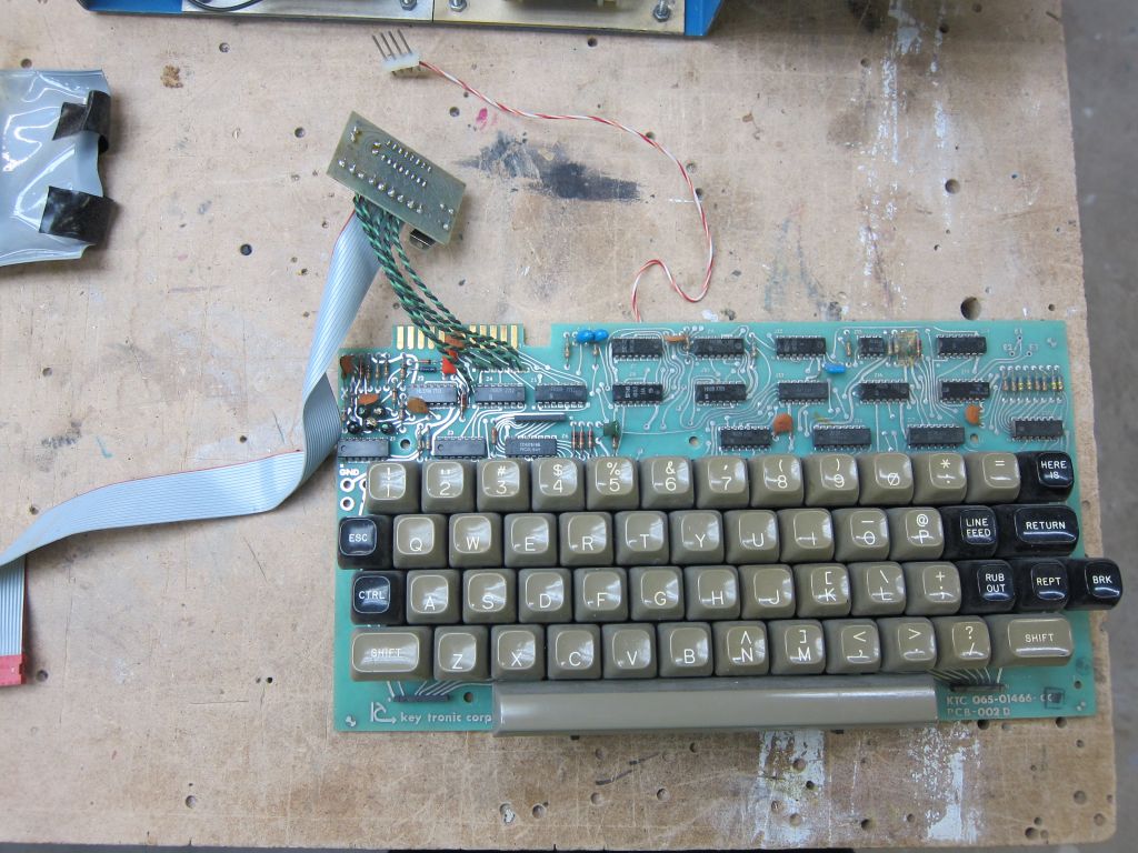
The Keyboard
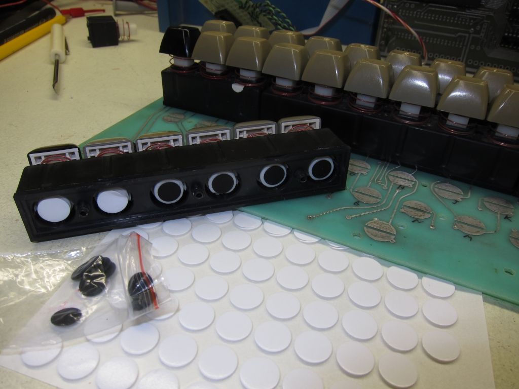
The oddest feature of this machine is the keyboard. Almost every (late 1977 and on) challenger 2 machine uses an OSI 542 polled keyboard, consisting of an 8×8 key matrix, an 8-bit latch and an 8-bit input port with the matrix scanned by firmware in the system ROM on the main CPU. By 1978 OSI was advertising the “C2-4P” machine using such a keyboard and supporting both upper- and lower-case characters. This particular primitive unit uses a Keytronic 65-1466 keyboard designed for ASR33 emulation. This Keytronic keyboard is not polled by the CPU but instead produces a strobe and parallel data read by the machine via a single byte-wide I/O port at $DF01 – the strobe is on the high bit (D7) and the lower seven bits are the ASCII data representing the key. In order to accommodate the keyboard a specific ROM must be used in the CPU board with machine-code routines to check the port.
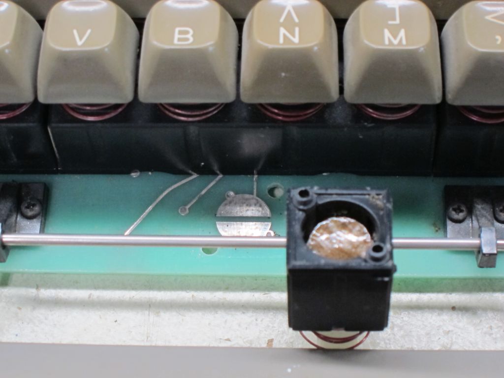
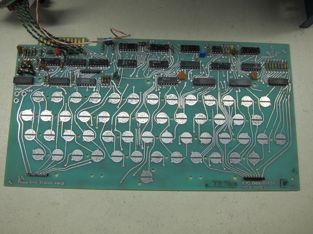
The keyboard used here is a Keytronics KTC-065-01466 (http://www.bitsavers.org/pdf/keytronic/). The keyboard is self-clocked and scans a matrix of 53 keys using discrete logic chips until a keypress is detected. The original keyboard was capacitive where pressing a key pushed a conductive mylar film against pads on the PC board coupling a 500KHz signal to a detector circuit. The original mylar film and foam pads were completely disintegrated – keys were removed from the PCB and all foam removed. Three self-adhesive foam pads (10mm in diameter, 1mm thick) were stuck to the key plunger and on top of that a 10mm piece of conductive rubber (made specifically for keypad repair). Three foam pads were required to ensure the conductive rubber pad actually touched the contacts.
The repair worked quite well however the keyboard still worked only occasionally. The circuitry was then diagnosed by checking all main circuits with an oscilloscope as follows:
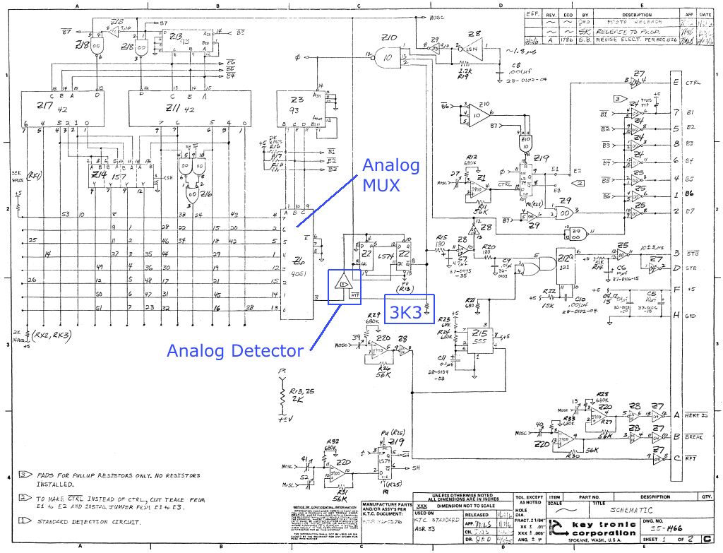
- Binary counters Z3&Z13 were verified: Z3 Pin 14 is clock in, outputs are 9,8,11. Z13 outputs are 12,9,8,11.
- Decimal outputs on decimal decoders Z11&Z17 were verified
- The analog MUX Z6 (4051) was verified to have output on pin 3 when a key was pressed
- Finally the detector circuit was verified – Keytronics even issued a procedure to diagnose problems with that circuit which uses five discrete transistors and this was, apparently, a common problem
Those tests verified the majority of the keyboard logic including key matrix scanning and key detection.
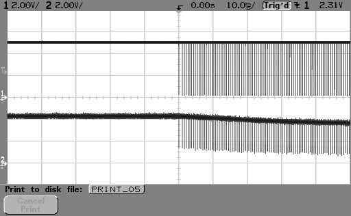
Now the signal from the detector circuit then latches Z2, a 74LS74 flip-flop (clocked by the oscillator) which then triggers a 74LS123 one-shot to generate a 10ms strobe pulse. Signals from the flip-flop output looked correct UNTIL a more careful examination showed the “logic low” level was only 1.0V … not low enough to register as “0” (0.8V for TTL). A 3K3 resistor was added to help pull the flip-flop output to a lower level and Voila! the keyboard began working as expected. So the chip did not simply fail as expected but rather became ‘weak’ and unable to sink the required current to drag the level low enough. (Yes, the 74LS74 should be replaced but I will reserve that for a future failure).
In the process of diagnosing the keyboard I discovered many things – this specific Keytronics model is an electronic clone of an ASR33 teletype and as such the layout is quite different from a modern keyboard. It also lacks lower-case capability (as the teletype did) – pressing SHIFT+L gives a backslash character but SHIFT+A still gives an uppercase A. Also evident is an odd layout where characters above each number ‘1’ to ‘0’ are different than a modern keyboard, e.g. this keyboard maps ‘(‘ above the 8 and ‘)’ above the 9 primarily as there is only one bit difference between the two values (so pressing SHIFT simply sets the fifth bit low for the special character) – that trick was used by the original teletype which used mechanical encoders as well.
Of course pressing two keys at once will only register the first key in the matrix as it is sequentially scanned column-by-column and was likely the a major reason OSI went with a polled keyboard for all later machines (detection of multiple keys being required for games).
Photos of the Keyboard rebuild …
Video
Considering the ASR keyboard did not support lower-case characters (I guess Word Processing wasn’t a thing for this machine), the 540 video card used did support these characters as well as gaming characters. On boot-up the machine is in 32-column mode. POKEing $DE00 (56832, the video mode register) with ‘1’ puts it into 64 column mode (possible since the card has 2K of video RAM). Subsequently, POKEing a ‘0’ changes back to 32 column mode.
Lines are 64 bytes in length regardless – in 32 column mode only the first 32 characters are displayed with the next 32 off-screen.
This older 540 board resembles the hardware used in the A revision board (with the exception of how it was used in this system to interface with the ASCII keyboard) including two sockets for a choice of character generator: one supporting only 64 characters with six-bit addressing and the other 256 characters as seen here.
Power
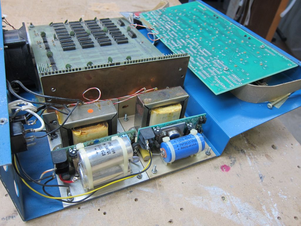
The system has two power supplies, a large one supplying +5V and a smaller one supplying -9V. The -9V supply is required by the CPU board for both the 1702 256-byte EPROMs as well as RS-232 mark voltage (if such a port is installed).
The main 5V power supply has no markings and uses the same PCB as the -9V supply however with heavier components such as the diodes, resistors, and power transformers (the 5V supply transformer has a center tap).
Two MR756 diodes (rated at 6A) and a Solitron PP3589 power transistor rated at 80W. Implies the supply is limited to an output of about 5A at 5V
The required power for the system boards is as follows:
500 CPU w/4K – needs 2A at +5V plus 500mA at -9V
420 Memory w/4K – needs 600mA to 1A (max) at +5V
If we assume the 540 video card consumes a maximum of 1A then 4A is needed for the three-board system.
As received, the unit had the usual leaky electrolytic capacitors which were replaced. The power supplies were then tested under load using large resistors to load them to maximum current before re-installing boards into the backplane. The main 5V supply operates quite warm.
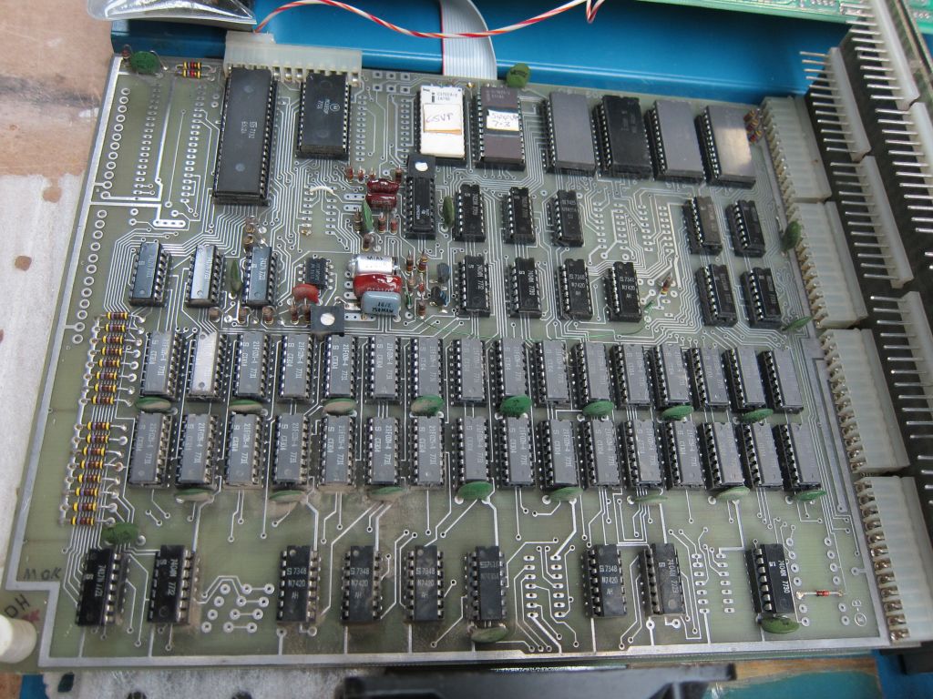
An Updated (1978) System
In 1978 OSI shipped an updated C2-4P which included a 502 CPU board, a 540 video card, and a polled keyboard. Only two slots in the four-slot backplane were occupied leaving room for a 470 floppy controller and 527 memory board for upgrade to a floppy-based system athough OSI shipped the “4PMF” floppy-based version with a 505 CPU which lacks on-card RAM altogether but features a disk controller on the CPU card. The “MF” system usually consisted of a 505 CPU, 527 memory board (24K), and 540 video card leaving one slot remaining for expansion.
The 502 CPU card, shown here as the top card in the backplane, features five ROMS (four for BASIC as well as one for the monitor, just like the superboard) and 8K of RAM in the form of sixteen 2114 chips. The CPU board also contains a 6850 ACIA as well as the associated analog circuitry used for the cassette interface. Note also that the system has only a single 5V power supply – without the 1702 EPROMs there was little need for a -9V supply.
This system, received in late 2008, had the usual bugs expected with an older machine including power supply issues in the form of failed electrolytic capacitors as well as a failure in one (or more) of the upper 4K of RAM chips. The on-board RAM was clearly expanded after production as the upper 4K are manufactured by a different company than the lower 4K (which was presumably installed by OSI). Removing the upper 4K of RAM allowed the system to boot.
The 502 CPU has a 2K monitor chip replacing multiple older 1702 EPROMs which actually contains eight individual segments of code including a 65V monitor, BASIC support, and a floppy disk bootstrap (it is labelled “SYNMON”). As shown here, the machine only presents a “C/W/M ?” boot prompt (logical since the CPU card has BASIC ROMs and was intended as a cassette-based machine) however the CPU has a unique priority encoder scheme using a 74148 allowing jumpers to map any code segment from the ROM into $FFxx, $FExx, and $FDxx in the memory map. The 2K ROM contains a floppy bootstrap for 5.25- and 8-inch disks as well as support for various systems, even a “440 style” ASCII keyboard on the older machine above.
With a newer 540 Video card a 64-character display appears on boot-up. A simple POKE command allows the user to switch between the default 64-character wide display and a 32-character wide mode, presumably for software compatibility with many games.