Presented is both the hardware and software for a Win-32 based Logic Analyzer which uses a multithreaded Win-32 front-end and a native USB interface.
Introduction:
When your hobby is collecting old computers (including a few 6800 processors on old arcade machines), a logic analyzer proves invaluable to diagnose a multitiude of problems. This particular project is a blend of hardware, both discrete logic and microcontrollers, and software in both assembly code and C++. The actual analyzer was inspired from the original article “High Speed Logic Analyzer for Windows 95” appearing in Circuit Cellar Dec. 97 pp. 46 by Francis Deck. The basic system uses a special FIFO chip (7204) which is dual-ported to store logic-state samples which are transferred into a PC and displayed using a Win-32 front-end. The original analyzer hardware, built back in 1998, featured a front-end written in BASIC and using the parallel port for transfer however there are many shortcomings to this approach. In this updated project a multi-threaded Win-32 front-end was written allowing good user control of the hardware. The system shown here features a 50MS/s sample rate, 4K sample depth, a trigger system to start sampling on a rising or falling edge on any particular channel, 3.3V and 5V logic family compatibility, and a high-speed native USB interface.
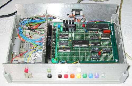 The logic analyzer hardware is packaged in a plastic box. Coloured tip-jacks on the front correspond to individual channel inputs with several extra jacks for auxiliary trigger inputs and outputs.
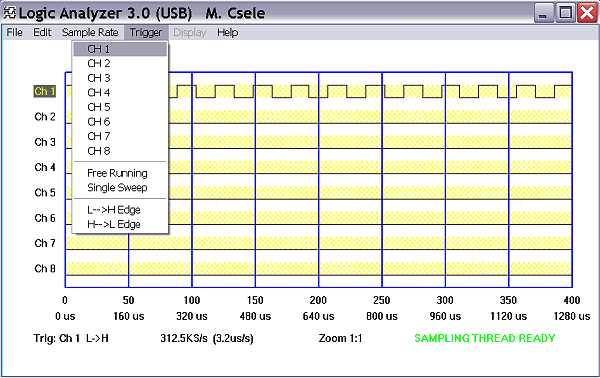
A front-end runs on Windows. A screen-shot of the Win-32 front-end for the analyzer (an older version 3.100) is seen here. Eight traces are shown on the wide display (optimized for a 1024 * 768 display). Pull-down menus allow the user to select sample rate, system voltage, trigger source, and other parameters. The sampling thread status is shown in the lower right corner – this indicates the status of the USB connection as well. Only 400 samples are shown on the display, but use of the arrow keys allows a left/right panning of the display to see all 4096 samples in trace memory.
Hardware and Firmware:
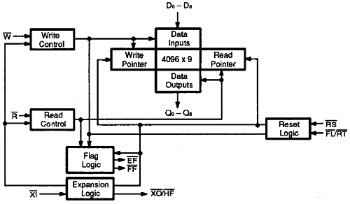 The key element of the analyzer is the AM7204 FIFO chip. This is a 4K dual-ported RAM chip which has separate read (Qx) and write (Dx) data paths. Each data path also has an address counter. To sample logic states into the chip, one first resets the counters via the /RS line and then provides clock pulses to the write clock (/w) on the chip at which point logic states on the write bus inputs (Dx) are stored into the chip. When the FIFO is full, a ‘buffer full’ signal (/FF) is asserted from the chip. To read from the chip, one supplies a read clock (/R) – on every pulse the chip transfers a byte from the memory to the read bus outputs (Qx). Like the ‘write’ cycle, 4095 clock pulses are required to read all 4096 bytes. Refer to the AMD datasheet (P/N 14430) for full details and timing of the chip.
While the original version featured direct control of the FIFO chip via the parallel port of the PC, this updated version uses a PIC18F4550 microcontroller to communicate with the PC via a USB port and controls hardware functions including sample clock rate, read clock (to read stored data from the FIFO), and trigger source. The actual sample clock is provided by a 50MHz crystal oscillator divided into many frequencies using a 74HCT4040 CMOS counter (earlier versions used a 20MHz oscillator as limited by the speed of the FIFO chip – the latest version uses a faster “L12” chip which operates much faster than previous versions). This provides the following sample rates: 50MS/s, 12.5MS/s, 3.125MS/s, 780KS/s, 195KS/s, 48.8KS/s, and 12.2KS/s. These rates can be changed by rewiring the counter outputs (and using a different crystal oscillator) but were chosen since each sample rate is four-times slower than the last.
Through the main interface the analyzer may be placed in an idle condition, reset, enabled for sampling, and data read from the FIFO. The idle (non-running) condition is asserted by bringing the enable line high (disabling clocking), reset line high, and read clock line high. Reset is effected by toggling the reset line low then high again. Data sampling is started by selecting a clock rate (via a 74HCT151 multiplexer) and enabling the clock by bringing that line low – triggering may also be selected first if used. Finally, reading data from the FIFO is accomplished by resetting the FIFO chip again, which resets the read pointer to zero, and toggling read clock which places data from the FIFO onto the ‘Q’ outputs of the chip (which are then read by the PIC).
One possible planned upgrade (not implemented yet) is a pattern-match trigger can be implemented using a 74HCT688 which will trigger sampling when a pattern appears (e.g. when connected to a data bus and the ASCII letter “A” {1000001} appears or to match a condition on several enable lines which must occur simultaneously). For the pattern-match trigger, it is planned to upload the pattern to a 74HCT595 serial-in latch using control lines then have the match condition trigger the analyzer via the eighth channel (so that “channel 8” trigger source is no longer available). One could even use “>” and “<” conditions provided by the ‘688 as trigger sources as well if required (although the ‘equal’ condition is by far the most useful).
The discrete circuitry was constructed on a 44-pin plug-in proto board with a ground plane on the top for noise immunity. The original board had several unused areas which are now populated by a 18F4550 40-pin microcontroller for the USB interface, and an area reserved for future expansion of several discrete logic chips for the pattern-match trigger. A USB jack is installed in the rear beside the original DB-25 connector for the parallel interface already in place.
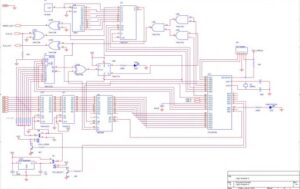 The Schematic for the latest version can be found here (in PDF format). An RJ-12 connector is permanently installed on the board allowing quick upgrades using an ICD debugger … when unused the connector is simply disconnected and tucked-into the case. Pins RB6 and RB7 are unused for any other purpose.
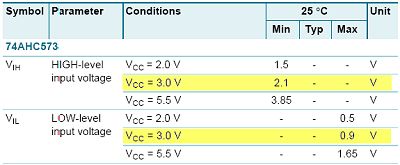 A 74AHC573 is used as an input buffer allowing 3.3V operation and two relays (driven from RA0 and RA1 on the microcontroller) select Vcc (3.3V, by default, or 5V) and either a pull-up (to Vcc) or pull-down (to ground) function for all unused inputs. The 74AHC573 was chosen since it has a very minimal propogation delay, can operate from 3.3V or 5V, and even at 3.3V can tolerate 5V inputs. The actual logic levels are defined such that at 3.3V they correspond to true TTL levels (ideally, 0.8V for low and 2.0V for high are true TTL levels but the AHC573 operating on a 3V supply has levels of 0.9V and 2.1V accordingly – see the excerpt from the NXP, formerly Philips, datasheet to the right). When 5V TTL logic is selected as the target supply level, this chip is actually run at Vcc=3.3V for true TTL compatibility, and only when CMOS 5V logic is selected is the Vcc of this chip brought to 5V (at which point the chip has logic transitions at 1.65V and 3.85V and so is MOS compatible). Even with a 3.3V supply, the output level of the AHC573 is still 2.9V minimum for a logic “high” (and 0.1V maximum for a logic “low” output) and so it is still TTL compatible and can drive the input of other chips in the circuit which are powered from a 5V supply such as the 74HCT573 already in the circuit (or the FIFO, directly, for that matter). Note that only the 74AHC573 version can do this trick: the HCT version (as used on previous versions of the logic analyzer) is strictly 5V only with logic levels of 2.0V and 0.8V – choice of logic family (and examination of the details in the datasheet) are crucial for this project. A common LD1086 regulator (in a TO-220 package) is used for the 3.3V regulator – an input of +9V is required for this regulator (+5V is not sufficient to ensure 3.3V output).
As far as speeds go, it is important that all chips be fast enough. The existing 74HC573AN (U4, from previous versions) has a 40ns typical propogation delay, the existing 74HCT251N has a 19ns delay. This is a good situation since, in essence, the 573 acts as a delay allowing the trigger signal to “catch up” with the signal at the data lines of the FIFO. For this reason, the new AHC573 was added in addition to the existing HCT573. Finally, the 74HC4040N is rated at 79MHz so operation at 50MHz is allowed.
Port D on the 18F4550 is used to input data from the FIFO in 8-bit parallel format (in the original version a 74157 selected four bits to read via the parallel port). Port B handles control lines to set sample rate and enable the clock, and Port C handles control lines for trigger source selection.
The basic USB firmware utilized is Nick Christoudoulou’s interrupt-driven implementation of Bradley Minch’s assembly language USB framework. The 18F4550 is configured with only a single control pipe (EP0) and all data is passed through this interface. Messages from the PC are sent as vendor-specific requests. In addition to a command, two 16-bit parameters (wValue and Index) are sent – in the case of this project, wValue contains configuration information for the analyzer (sample rate, trigger channel, etc). Commands are defined as follows:
CMD_IDLE: idles the hardware (no sampling)
CMD_RESET: resets the FIFO counters and trigger FF
CMD_START: starts the analyzer with parameters specified in wValue
GET_FIFO_STATUS: returns a single byte describing the FIFO status (Full or Empty)
GET_FIFO_DATA: retrieves eight bytes of data from the FIFO vie the EP0 buffer
The CMD_START command accepts a single 16-bit word as an argument in which the bits are assigned as follows:
Bits D0-D2 define the Sample Rate (000=ext, 001=20M … 111=4.9K)
Bits D3-D6 define the Trigger Channel (0000=Free, 1-8=Channel#, 9=Pattern selected)
Bit D7 sets the trigger edge (with 0 signifying a Low-to-High edge)
Bit D8 defines Vcc (0=3.3V, 1=5V)
Bit D9 defines Pullup or Down of unused inputs (0=pull down, 1=pull up)
For commands where a value is sent from the PC to the analyzer, the parameter is sent on wValue which is extracted from the incoming USB buffer as follows:
movf USB_buffer_data+wValue, W, BANKED
movwf ParmwValue1,BANKED
In reality, it is extracted as two 8-bit values since wValue is actually a sixteen-bit number from the PC. Bits, which represent individual values, are then extracted. For example, Bits 0-2 of wValue are extracted then sent to PortB as follows:
andlw b’00000111′
iorlw b’00111000′ ; Ensure Clk/Rst/Enable lines stay high
movwf PORTB
This code ensures that bits 3-5 of PortB stay high to disable clocking.
Where a value is to be sent back to the PC the value is written to the USB buffer and the endpoint control registers set to send the buffer back to the PC. In the case of the GET_FIFO_STATUS command FSR0 is first set to point to the EP0 IN buffer, the FIFO chip is tested (PORTE, FIFO_FULL line), and POSTINC0 is set to 0x00 or 0x80 to represent the FIFO status (hence only the first of the eight bytes in the buffer are used in this case). Finally, the buffer control registers are set to send 8 bytes and the UOWN bit is set allowing the USB SIE to take control of the buffer and send it to the PC (this is the single-bit system used to control access to the buffers):
banksel BD0IBC
movlw 0x08
movwf BD0IBC,BANKED ; set byte count to 8
movlw 0xC8
movwf BD0IST,BANKED ; send packet as DATA1, set UOWN bit
Only eight-byte data packets are sent back to the PC (the most basic allowed in USB). Larger packets could be sent to enhance transfer rates however it simply did not seem to be required for a project like this. This also means that a ‘serial USB’ chip could be used for the project instead of a native USB interface.
A single LED indicates the USB status with a constant ON indicating the device has been enumerated (this occurs after the PC recognizes the device, usually accompanied by a “bing bong” sound effect) and Blinking indicating the device has been configured (which occurs when the front-end software is run and actually opens the USB channel for access). The LED is the only task which runs in main and this same LED is used as the unit power LED (so that “power” is actually “status”).
The USB portions were verified using a Beagle-480 protocol analyzer. The project was built with MPLAB version 7.50 and 8.43 and a linker script (for the 18F4550) is required (18F4550_g.lkr in 8.xx). Other required files include 18F4550.inc (from MPASM) and two include files from the original framework.
Downloads (Hardware):
Software elements (PC Side):
The actual data acquisition (i.e. the interface between the hardware and the PC) is handled by a thread which runs continually. On command from the Win-32 front end (via a semaphore), the thread begins data acquisition. When the FIFO is full, data is read into a global array and a message is sent to the Win-32 front end to force a PAINT and redraw the screen (along with new data read from the analyzer). Synchronization between the front-end and the thread, then, is accomplished via a semaphore and a Windows message (DATA_RDY).
To prevent the thread from ‘hanging’ when an unused trigger channel is selected, the current trigger channel, trigger edge, and sample rate are saved immediately before data acquisition takes place (and before parameters are sent to the logic analyzer hardware). During a wait for the FIFO, these parameters (all global) are compared to the start parameter – should any change the analyzer will be reset and data acquisition will be restarted. The user, then, always maintains control of the acquisition thread even while it is in a loop waiting for the FIFO to fill. The basic algorithm, running in the data acquisition thread, looks like this:
while(ParameterChange==TRUE)
{
//Save start parameters to detect change during data acquisition
CurrentSampleRate=SampleRate;
CurrentTriggerChannel=TriggerChannel;
CurrentTriggerEdge=TriggerEdge;
ParameterChange=FALSE;
//Send START_ACQUISITION command to start logic analyzer
ret = usb_control_msg(… , CMD_START, …);
//Wait for FIFO to fill — Don’t do this in a Win-32 proc
FifoFull=FALSE;
while (FifoFull==FALSE) //Input(InputAddress)&FULLFIFO)
{
//Check Fifo status
ret = usb_control_msg(… , GET_FIFO_STATUS, …);
if (buffer[0]==0x80) //Check the EP0 buffer returned from the device
FifoFull=TRUE;
if(CurrentSampleRate!=SampleRate) {
ParameterChange=TRUE;
break;
}
if(CurrentTriggerChannel!=TriggerChannel) {
ParameterChange=TRUE;
break;
}
if(CurrentTriggerEdge!=TriggerEdge) {
ParameterChange=TRUE;
break;
}
} //while FifoFull
} //while ParameterChange
The usefulness of a thread is evident here: it would not be possible to have a loop which continually checks for user changes. It might be possible to use a timer to implement this, however a thread is certainly the most convenient (and the code was already implemented for the previous version so only minor changes were required when adding the USB port).
Next, the semaphore is created to synchronize the thread:
hSyncDAQ = CreateSemaphore( NULL, 0, 1, NULL );
the semaphore is released in the main program and causes the thread to halt until released via a ‘WaitForSingleObject’ within the thread itself. The advantage of this is that while waiting, the thread does not consume copious quantities of CPU time! This requires that the thread possess the handle to the semaphore – currently this is done via a global variable however it could have been passed to the thread when the thread was created, since CreateThread allows passing of a parameter.
Upon receiving a WM_COMMAND, parameters such as sample rate are updated from the menu. When a port is selected via a menu option, the hardware is checked at that I/O address and if functioning, the data acquisition thread is started – this prevents attempt to access non-existent hardware. To test the hardware, the system is set for maximum sampling rate, free-running (no trigger), and the FIFO chip is reset. The Buffer full line (active low) should be high since the buffer is now empty (if not, the hardware is not functioning). The analyzer is now allowed to run for 1ms. In about 0.2ms, the buffer (after 4095 clocks) will fill and the buffer full line should go low – if it is, the hardware is now deemed to be operational. This is, BTW, a bit of a hack since inserting a ‘Sleep(1)’ command within a windows procedure is generally not a good idea (although it is, at least, predictable and will never wait indefinitely). Because this is only done rarely (only when setting the port initially), it is tolerable here (although using a proper windows timer would likely have been the best ‘textbook’ solution).
As usual with a Windows program, all screen draws are done within the WM_PAINT message section. Within this section lines are drawn to demarcate the grid, text is drawn to label the grid, current system parameters such as sample rate are drawn on the screen, and traces are drawn for each channel. Drawing traces was a bit tricky since vertical lines must be drawn at each transition. After the entire screen is completely redrawn, the semaphore is released allowing the thread to acquire a new set of data to draw … releasing the semaphore only after the PAINT is complete prevents the data acquisition thread from generating messages faster than the screen can redraw them (it was also found necessary to limit the number of times per second the thread can run regardless to prevent the image from updating too quickly to prevent being read).
The most recent updates to the program include a COPY to clipboard feature allowing screen outputs to be saved in any graphics program. Previously, the user was required to press the “PrtSc” key and the paste the image into a graphics package – the Copy feature saves this step. Other added features include the ability to pan through samples using arrow keys allowing all 4000 samples to be viewed.
USB Interface
Upon WM-CREATE, the code searches for a USB device matching the VID and PID specified (it must match that used in the PIC firmware, in this case VID=0x04D8 and PID=0x0004) returning a ‘usb device’ handle udev. The code then sets the configuration, claims the interface, and calls are made to transfer data to/from the USB device as per the following examples:
ret = usb_control_msg(udev, USB_TYPE_VENDOR | USB_RECIP_DEVICE, CMD_RESET, 0, 0, buffer, 0, 100);
This call sends a vendor-specific command ‘CMD_RESET’ to the device. The buffer is unused in this case as is wValue (parameter #4), either of which could be used to send data to the USB device.
ret = usb_control_msg(udev, 0xC0, GET_FIFO_DATA, 0, 0, buffer, 8, 100);
This call issues the GET_FIFO_DATA command. On completion of the call eight bytes of ‘buffer’ will be returned with eight consecutive samples from the FIFO.
Downloads (PC Software):
The USB library files include an INF file as well as several drivers. Unzip the files into a directory and when prompted for a driven when the device is connected, look for files in that directory (Windows will find all required drivers there). These files are a subset of version 0.1.12.0 of the LibUSB-Win32 project on sourceforge.net and are provided in the interests of simplicity only: for the current version of the LIB-USB driver, look for updates on sourceforge. This is an open-source project covered by the GNU licence and so the drivers are free.
To install the USB drivers, simply run the installer from the sourceforge project (libusb-win32-filter-bin-0.1.12.2.exe), plug the device into your PC, and install drivers when prompted. Be sure to run the testlibusb.exe program included with the driver (in the zip file as well) and ensure the logic analyzer appears there (with the correct VID and PID) before trying to run the LogicAnalyzer executable. If the drivers are not properly installed, the logic analyzer will always respond with an error (“No matching USB device found”). So long as the test program reveals the device, it should work. Upon starting the logic analyzer you will see a red error message in the lower-right corner of the window until the thread starts and communications is established after which the message turns green and states that the sampling thread is ready. Should an error occur, several message boxes detailing errors will be shown after which the program will sit dormant in an inactive state (it will not, however ‘hang’ and so can be terminated normally).
USB Demystified …
USB can seem mystical, but with the benefit of a protocol analyzer (in my case a TotalPhase Beagle 480), allow me to present the process of USB transfers in a simplified manner by demonstrating how the logic analyzer accomplishes communications with a PC.
The USB transfer process begins with enumeration in which the device is assigned an address by the host PC. Once detected upon plug-in, the PC sends the device a request for the device descriptor:
	Get Device Descriptor (64 bytes)
		  SETUP 2D 00 E8
		  DATA  C3 80 06 00 01 00 00 40 00 DD 94
		  ACK   D2
This request is directed to “device 00”, our logic analyzer which is unassigned right now. The device (analyzer) responds with a description. Even though 64 bytes (max) were requested by the PC, the device sends back only eight bytes as follows which describe the device as a USB 1.1 device with an 8-byte maximum packet size:
	  IN txn
		  12 01 10 01 00 00 00 08
The actual transfer looks like this through the protocol analyzer’s eyes:
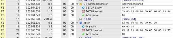
Here we see the request from the PC for the descriptor and the 8-byte response from the PIC in our logic analyzer. The actual bytes sent are simply a table in the PIC as follows:
	db	0x12, DEVICE		; bLength, bDescriptorType
	db	0x10, 0x01			; bcdUSB (low byte), bcdUSB (high byte)
	db	0x00, 0x00			; bDeviceClass, bDeviceSubClass
	db	0x00, MAX_PACKET_SIZE	; bDeviceProtocol, bMaxPacketSize
	db	0xD8, 0x04			; idVendor (low byte), idVendor (high byte)
	db	0x04, 0x00			; idProduct (low byte), idProduct (high byte)
	db	0x00, 0x00			; bcdDevice (low byte), bcdDevice (high byte)
The PC now instructs the USB device to become address 1 with the following command (when first started, the device has no address assigned and so responds to address zero):
	Set Address (=01)
		  SETUP 2D 00 10
		  DATA  C3 80 05 01 00 00 00 00 00 EB 25
		  ACK   D2
The USB device now responds only to address 1. The PC now requests the device descriptor again (this time, from address 01 seen in the setup portion of the packet sent from the PC as “2D 01”, and this time only 18 bytes are requested since the PC now knows the size of the descriptor packet from the first request):
	Get Device Descriptor (18 bytes)
		  SETUP 2D 01 E8
		  DATA  C3 80 06 00 01 00 00 12 00 E0 F4
		  ACK   D2
And the device responds with the entire 18-byte long descriptor in three packets (each with a maximum length of eight bytes):
	  IN txn
	    	12 01 10 01 00 00 00 08
	    	D8 04 04 00 00 00 02 02
	    	00 01
Next, the PC requests the configuration descriptor which describes how the device is powered as well as the interfaces it contains. First, the PC asks for 9 bytes then for the descriptor again, this time up to 255 bytes in length:
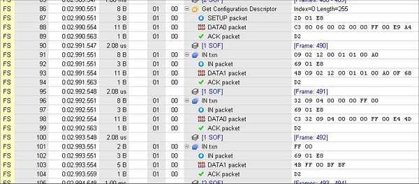
Once again, the descriptor packet is simply a series of bytes stored in a table in the PIC as follows which describes the interface including the class (in this case vendor, but in many cases a device may belong to a class such as communications or human interface devices such as a keyboard or mouse):
	db	0x09, CONFIGURATION	; bLength, bDescriptorType
	db	0x12, 0x00			; wTotalLength (low byte), wTotalLength (high byte)
	db	NUM_INTERFACES, 0x01	; bNumInterfaces, bConfigurationValue
	db	0x00, 0xA0			; iConfiguration (none), bmAttributes
	db	0x32, 0x09			; bMaxPower (100 mA),
					; bLength (Interface1 descriptor starts here)
	db	INTERFACE, 0x00		; bDescriptorType, bInterfaceNumber
	db	0x00, 0x00			; bAlternateSetting, bNumEndpoints (excluding EP0)
	db	0xFF, 0x00			; bInterfaceClass (vendor specific class code),
					; bInterfaceSubClass
	db	0xFF, 0x00			; bInterfaceProtocol (vendor specific protocol used),
					; iInterface (none)
Description strings are now requested by the PC which describe the device:
	Get String Descriptor (255 bytes)
		  SETUP 2D 01 E8
		  DATA  C3 80 06 02 03 09 04 FF 00 97 DB
		  ACK   D2
And the string describes the device as “Logic Analyzer ….”
	  IN txn
		    2E 03 4C 00 6F 00 67 00	;   L o g
		    69 00 63 00 20 00 41 00	; i c _ A
		    6E 00 61 00 6C 00 79 00	; n a l y
		    7A 00 65 00 72 00 20 00	; z e r _
		    33 00 2E 00 58 00 20 00   ; 3 . X _
		    55 00 53 00 42 00	; U S B
These strings are the ones which appear in the lower-right corner of the screen when a new device is plugged-into a PC. They are for identification to the user only. The PC can request the string, device, and configuration descriptors again as required.
Finally, the Configuration is set to 1 (normal for a single device):
	Set Configuration
		  SETUP 2D 01 E8
		  DATA  C3 00 09 01 00 00 00 00 00 27 25
		  ACK   D2
The device is finally ready, and data transfer can occur with the device. In the case of the logic analyzer, data is sent bidirectionally via a single endpoint (EP0).
USB Data Transfers
With setup complete, normal operation appears as per the following example …
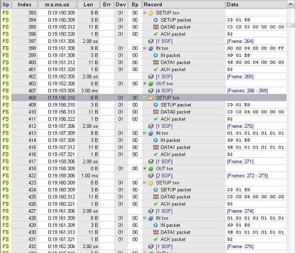 After configuring the analyzer (trigger channel, etc) and resetting it, the PC polls the FIFO status as seen in Index 395 above in which a “Get Fifo Status” command (03) is sent to the PIC. The PC normally must wait many such cycles for the FIFO to fill but in this case (Index 398/400) the FIFO is already full and so 0x80 is returned in the DATA1 packet. The front-end program on the PC the issues a “Read Fifo” command (04) at Index 408/410 and data from the PIC is sent to the PC in groups of eight bytes at Index 413/415 (seen here as all “01”s – it was a slow square wave on channel 1 only). The PC continues issuing ‘read’ commands and in response received eight data bytes from the FIFO. Data is restricted to eight bytes allowing transfer of data on endpoint EP0 at any speed (Low speed mode is the limiting factor here). One could open another pipe (e.g. EP1) to transfer the entire contents of the FIFO in one shot (i.e. all 4096 bytes) however the simple approach of a single pipe was used here (hence why the Beagle analyzer interprets the packet transferring data from the PC to the PIC as “SETUP txn” …. normally one expects data to be transferred via a different pipe than EP0).