Around 2010, MEMS (Micro Electro-Mechanical Systems) technology became available on the commercial market providing devices such as tiny (and inexpensive) accelerometers. An accelerometer measures forces applied to a test mass: in the case of a MEMS accelerometer, a test mass and support springs are manufactured on a chip using silicon with movement of the test mass detected using capacitance between the mass and fixed plates on the MEMS chip. I received one of these (relatively new at the time) chips as an engineering sample) and built a recording accelerometer primarily for recording motion on amusement rides (specifically at DisneyWorld as I am a bit of a Disney addict).
Hardware
MEMs Accelerometer
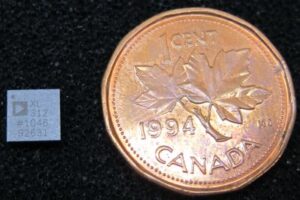 The accelerometer chip used in this project is the Analog Devices ADXL312 3-axis accelerometer which can measure acceleration in all three axes (X, Y, and Z) up to +/- 12g’s and with 13-bit resolution.
This chip is extremely tiny and supplied in a 32-lead package only 5mm square! It is seen here beside a penny for size comparison.
A primer on accelerometers can be found on Wiki.
To be practical, the ADXL chip is far too small to prototype in it’s existing package so it was mounted onto a standard 8-pin machined DIP socket used as a header. Thin wires attach the leads to the pins, soldered by hand using a powerful magnifying glass and an ultra-fine (0.2mm radius) tip on my Hakko soldering station. The “blob” of solder in the middle of the package is actually where a ground lead attaches to the bottom pad.
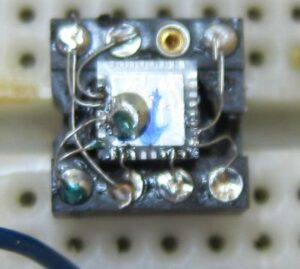 After attachment to the header, the entire assembly was covered with five-minute epoxy to protect the delicate connections.
Incidentally, it should be noted that the chip is actually mounted upside-down in this manner so that if it lies on a flat PCB, the ADXL chip will always read “-1g” instead of “+1g” (although this is easy to correct in a spreadsheet during data analysis and is not really relevant in usage anyway: the packaged version of the project includes three powerful magnets on the rear of the unit so that it can be affixed to a vertical surface in which case the X-axis will show “-1g” when stationary).
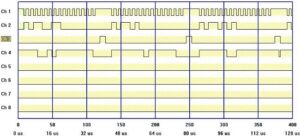 This project also helps illustrate the usefulness of a homebuilt logic analyzer. Here you see three SPI reads of registers (0x33, 0x34, and 0x35) in the ADXL chip (with SCLK on channel 1, serial data on channel 2, and chip select on channel 3) along with the chip response as seen on channel 4. During debugging, a faulty piece of code continually sent the same command (“read device ID” command) … the logic analyzer revealed the nature of this fault immediately.
Display
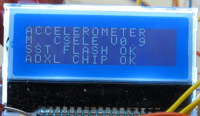
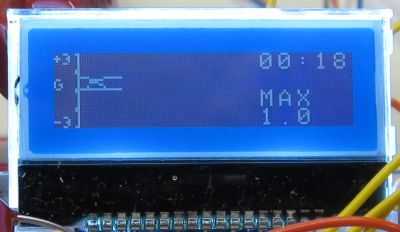
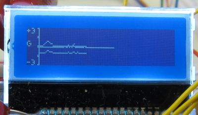
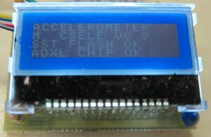 The device was designed to incorporate a small graphical LCD display – a Newhaven Display NHD-C12832A1Z-NSW-BBW-3V3. This chip-on-glass display is inexpensive, offers full graphics capability, and has an easy-to-use serial SPI interface. Many NHD displays use the same basic interface and so this project as a good excuse to write a library of basic functions for the LCD, as well as some high-level ones (including graphing). The only real downfall of this display is the fact that it requires eight external 1μF capacitors (which ultimately occupy board space).
Like the ADXL chip, the LCD was mounted on a 20-pin DIP socket as a header for prototyping as seen here – in the final version of the project the 1.5mm pin spacing (unusual) was far enough apart to allow thru-hole mounting directly on a PCB.
Other Circuitry
The original design was to use the on-chip flash memory of the dsPIC chip to store data (using the ability to write directly to flash program memory under program control as employed in other projects I’ve built using dsPIC processors) however the 128K offered was simply not enough and so an external flash chip was added. Microchip’s SST flash (a relatively new product) was used – the SST25VF032B offers 32MBits (4 MBytes) of storage, is packaged in a small 8-pin SOIC package, uses a serial SPI interface, and is quite fast.
The dsPIC33FJ128MC802 microcontroller employed has only two SPI interfaces (which is more than most devices which have only one and was one of the main reasons for using this particular chip) however three SPI devices are used on this design (ADXL, LCD, and SST flash memory). The ADXL uses a 16-bit mode while the other two devices use an 8-bit mode and so those two share the same interface (albeit with separate chip-select lines).
Finally, all chips run at 3.3V and the supply chosen was a tiny Olympus digital camera battery (operating at 3.6V) so a MAX882 low-dropout regulator was used. This regulator will supply 3.30V output with only 3.37V of input supplied! Circuitry is amazingly low-power, with a measured current drain of only 16mA with the backlight on, and 9mA when recording with the backlight off. Since it was recognized that the backlight will consume more power than the rest of the circuit, (a) the backlight current was limited to 7mA instead of the usual 25mA and (b) the backlight is controlled via an I/O line from the processor allowing it to be turned off during recording.
Complete Circuitry
The complete schematic can be found here. Not shown on the schematic is the RS-232 serial interface which allows data to be downloaded to a PC. That interface, on a separate board which plugs into the accelerometer when required, uses a MAX3223 driver chip which is similar to the ubiquitous MAX232 however operates at 3.3V and uses only 0.1μF capacitors. It features a shutdown mode as well to limit current drain when not in use however this is unused since the downloader interface is only plugged-in as required. The interface is powered from the accelerometer itself (the regulated +3.3V supply). Since all modern laptops lack a serial port, an RS232-to-USB bridge is used.
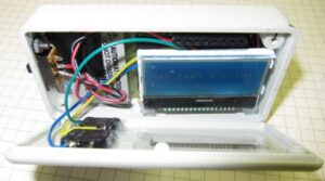 The download adapter installed, allowing data to be downloaded to a PC.
In this photo, the entire assembled unit can be seen with two user pushbutton controls, a rectangular window for the LCD, and eight holes for access to the I/O connector on the PCB (to which the male connector on the download adapter mates).
Data is downloaded to a PC at a rate of 115.2KBaud.
Packaging
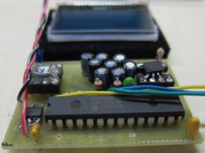 To keep the unit as small as possible all components were mounted on a small PCB on top of which the LCD is mounted. The through-holes on the nearest edge of the PCB are for the eight-pin I/O connector … holes for the LCD are on the opposite side of the PCB and so are not visible here.
Since many components are SMT, it would make sense to design the unit to allow direct mounting of such components on the board however for this prototype it was chosen to use the components already in the DIP adapter sockets, primarily because this was a “junkbox” project and so the only capacitors (and MCU) available were in through-hole packages. The tiny 8-pin SOIC chip to the left of the MCU is the MAX882 LDO regulator, mounted on top of the board using thin wires.
The PCB is housed, along with the lithium battery, in a small plastic box. Two thin pushbuttons glued to the top cover are used for user controls (increment and enter). These are recessed from the front surface to prevent accidental presses.
Once completed, the prototype unit showed severe noise: With the unit sitting stationary on the workbench the value for “-1g”, normally numerically around -350, varied up to 50 LSB values randomly. (Note that, as explained earlier, the chip is upside-down). The electrical noise was reduced drastically by adding both a 0.1μF capacitor across the power leads directly under the ADXL chip and another 10μF tantalum capacitor right beside the ADXL. The result is a reduction is noise by approximately a factor of five! When laying-out the PCB, be sure to include thick ground leads and adequate supply decoupling.
 The same PCB with the LCD mounted on top making a compact package containing all electronics as well as an I/O connector for connection to a downloader interface and ICD for reprogramming the dsPIC controller. The LCD is supported by two thick copper wires on the backlight terminals, as well as the seventeen small data wires. The limiting factor on how thin the unit could be built was the height of the capacitors (again, using SMT would allow a much thinner unit to be built and all components except for the display are available in SMT packages).
Software
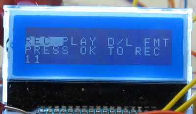
The code, written in MPASM, is relatively simple and includes a simple menu-driven system allowing the user to select basic functions. On format, all memory is cleared to 0xFF. When the record function is selected, the code looks for the first available memory slot (memory is separated into slots of 128K each) as identified by the first few bytes being 0xFF.
Samples are then taken and stored into flash as eight-byte structures as follows:
- Sequence number (two bytes)
- X-Axis value, 16-bits (two bytes)
- Y-Axis value, 16-bits (two bytes)
- Z-Axis value, 16-bits (two bytes)
The sequence number is used to identify the time of the sample, and ensure data integrity during download. All numbers are stored in little-endian, two’s-complement format. With a 128K memory slot, and a sample rate of 25Hz, each slot can hold just over ten minutes of data and a total of 32 such slots are available.
The LCD is graphical with a resolution of 128 dots across by 32 dots high. It is static, requiring no refresh signal, and features a simple serial interface with a basic command set allowing positioning of the write pointer to display memory, writing of display data, etc. When displaying text, it is logically arranged (in software) as four lines. Character generation is supplied by a lookup table derived from the video section of an old Ohio Scientific (circa 1979) computer.
The complete firmware can be found Here (as a zip file) (Version 1.1). It compiles under MPASM 8.xx IDE.
Testing
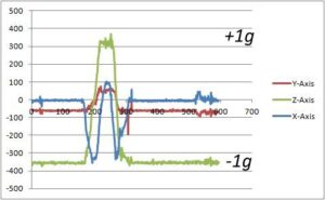 In this basic test, the unit starts by sitting flat on the workbench so that the Z-axis data (in green) reads around “-350” – the value for -1g in this axis (as noted earlier, the chip is upside down) – while the X and Y axes read zero. The Y-axis shows an offset error of approximately -60 caused either by the chip itself of from the unit not sitting completely flat. Offset can be set in the chip itself, or later during analysis by simply subtracting this constant from all values for that axis. As the unit was turned towards the rear, the acceleration measured by the Z axis decreases and that measured by the X axis increases. In this case, the entire board was turned upside down so the Z axis reading goes from -1g to zero (when the unit is on it’s side) and up to +1g when upside-down. The X-axis, on which the unit was turned, goes from 0g to 1g during the turn, and back to 0g when upside-down. The Y-axis should remain at zero, however and turning of the unit shows as increased acceleration. This indicates how the unit can actually be used as an inclinometer if desired.
The real test was to take the accelerometer to an amusement park – and there was no better place to do this than Walt Disney World in Florida! Outlined on another page is raw data from the accelerometer as well as analysis, including integration of the data to yield both velocity and positional data, for rides such as the Twilight Zone Tower of Terror, Mission Space, and others.
The accelerometer alone has limitations, though, as it cannot identify the axis in which acceleration occurs. In order to identify the direction as well, a gyroscope is required. MEMs gyros are now available in tiny packages as well – adding one to this project would certainly enhance the functionality of the system and allow determination of direction at any point in free space.
